Analogue IC Design
slides:https://pipirima.top/2022-2023/Analogue-IC-Design-Slides-ee210f4e9f8f/
Introduction
The previous several slide is almost same as the slids in undergraduate and been ignored.

Normally in real manufactory, there have two more taps placed on two sides of MOSFET, in order to avoid body effect and let MOSFET works more like a FET.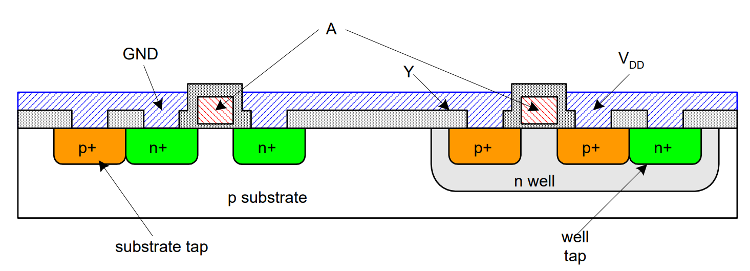
A MOSFET device with multiple view directions: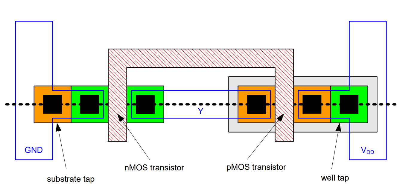
Development of FET:
Transistor -> LOCOS -> STA -> High-K/Metal gate -> FinFET -> RibbonFET
Chips are made my many wires called “Interconnect” which influences the speed, Power, and Noise in chip.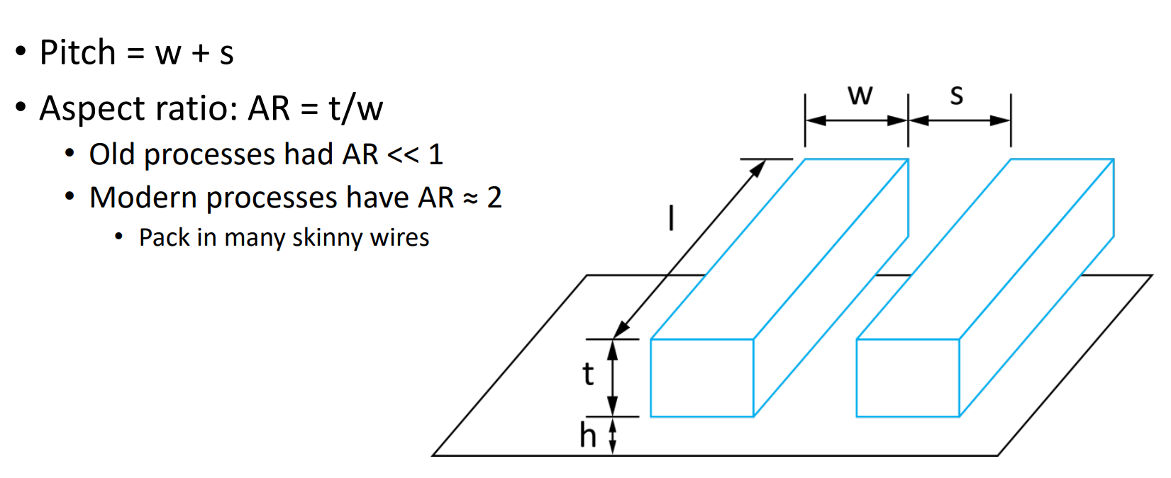
There have three types of wires used in chip design
M1 for within-cell routing
M2 for vertical routing between cells
M3 for horizontal routing between cells
More deeper the chip is, Much thiner and narrower the wires is.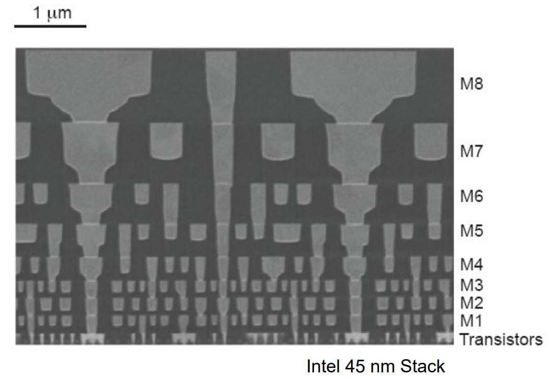
For packaging, Ball-Wedge gold wire for low currents and Wedge-Wedge aluminum for high currents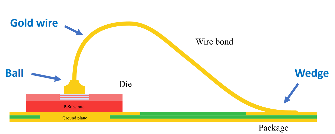
FET theory
A FET(filed-effect transistor) is worked based on generated channel between source and drain terminal (by the effect of applied voltage)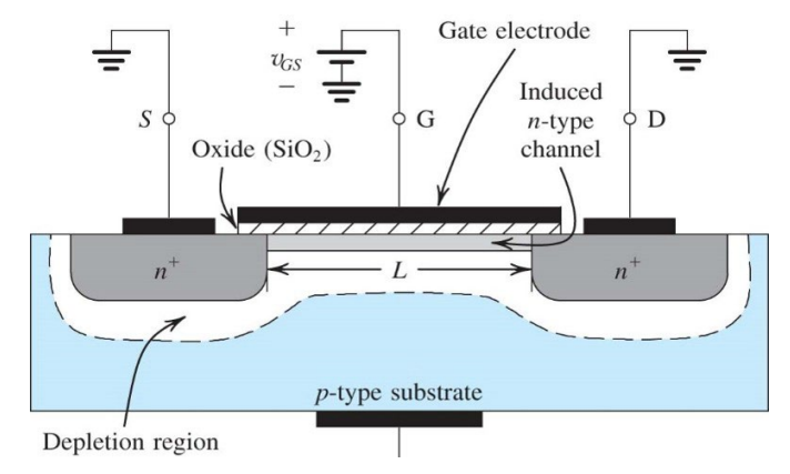
Normally the VT for n-mos is 0.3-1.0 V. Opposite value for p-mos
Quantity of charge in the channel is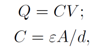
where C is capacitor and A is area, d is distance
And Cox=εox/tox, tox is thickese of oxid, εox= material permittivaty*ε0, ε0=8.854 E−12 F/m
Normally N-mos is better than P-mos as electron mobility if nearly 2-4 higher than holes. hence N-mos can be switched much faster.


Kn is the MOSFET transconductance parameter

the id and rds can only used on VDS is small number
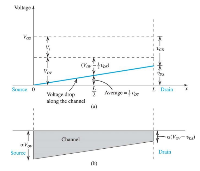

the final channel width is influenced by VDS. this figure is shown cases when Vov>VDS (non-saturation)
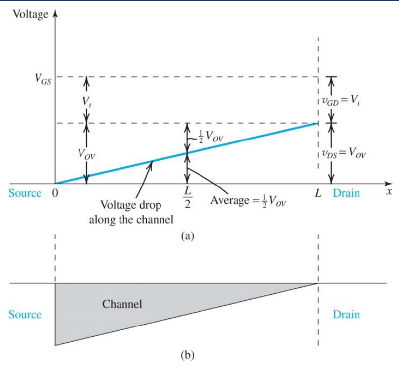

and the final channel width will completely disappeared (pinch-off) when VDS>Vov (saturation region)
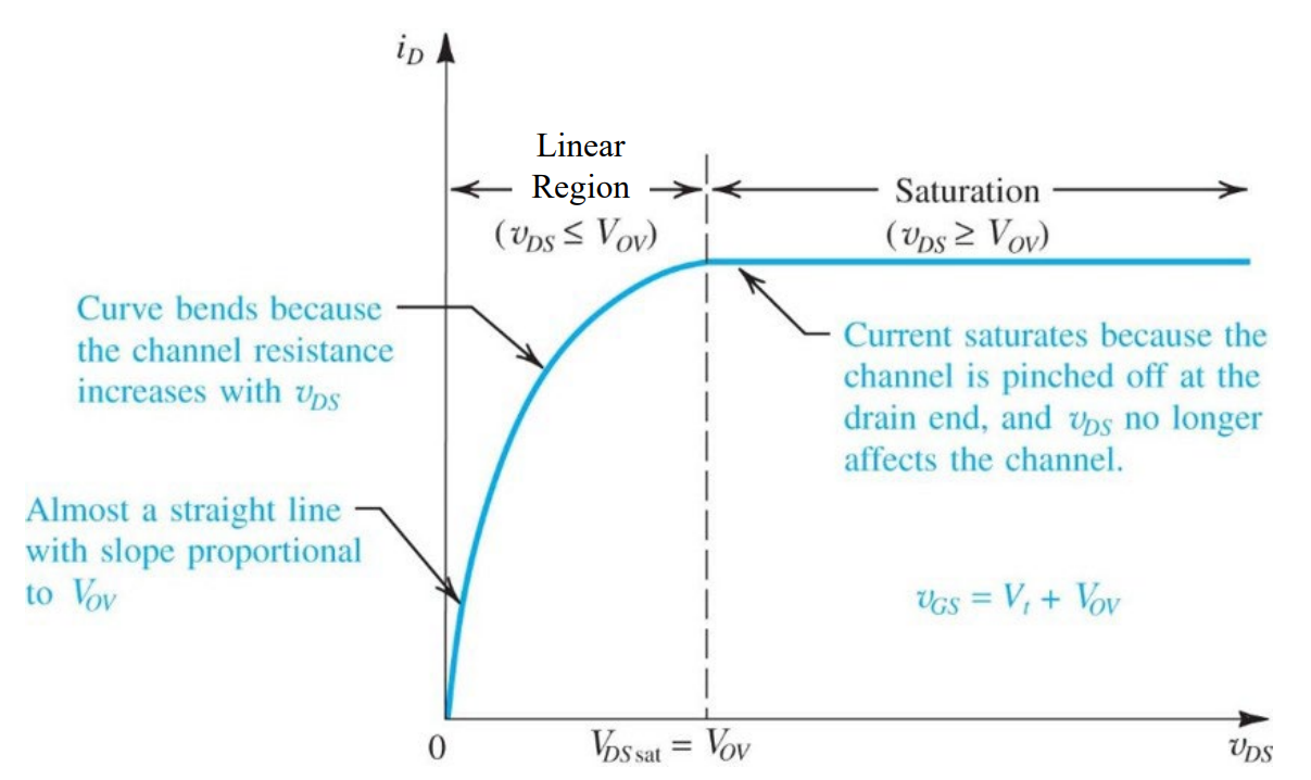
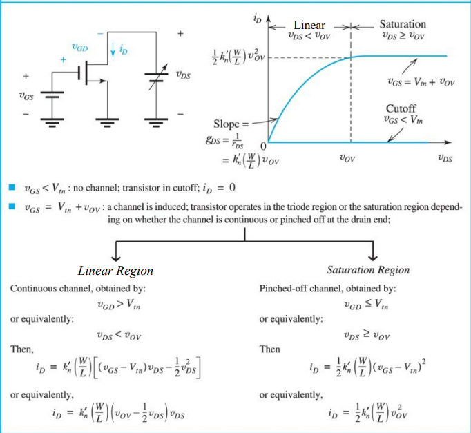
The output resistence r0 for saturated transistor is inifite, but in practice, increasing VDS beyond Vov does affect the channel. As VDS is increased, the channel pinch-off point is slightly moved away from the drain towards the source. which is called “channel-length modulation”.
the slop in channel-length modulation is = 1/r0 = (1+λVDS)/λID = 1/λID
with “channel-length modulation” :

the body effect is happened when the voltage drop on body terminal is not equals voltage on source.
Normally will influence Vth voltage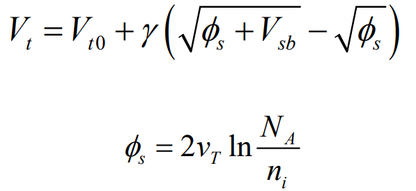
FET amplifiers (part1)
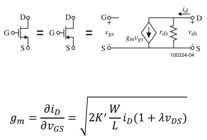
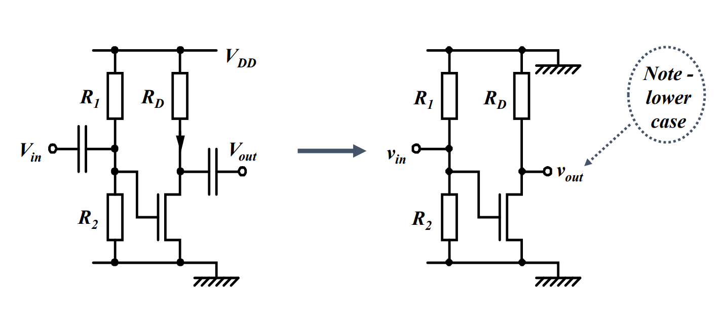
Signal analysis steps
- small signal can only use in AC analysis
- set all DC voltage in zero
- large capacitor becone short
- analyse using Ohm’s Law and Kirchhoff’s Laws
- get gm and rds
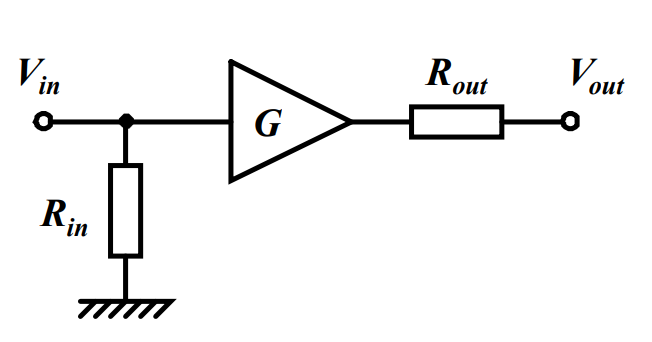
this the the most useful amplifier module
Rin is the amplifier inputimpedance (usually infinite for perfect MOS circuits)
Rout is the amplifier output impedance
G is the amplifier gain, usually negative
the ideal transistor plot in saturation region should be a linear current mirror for both p-type and n-type transistor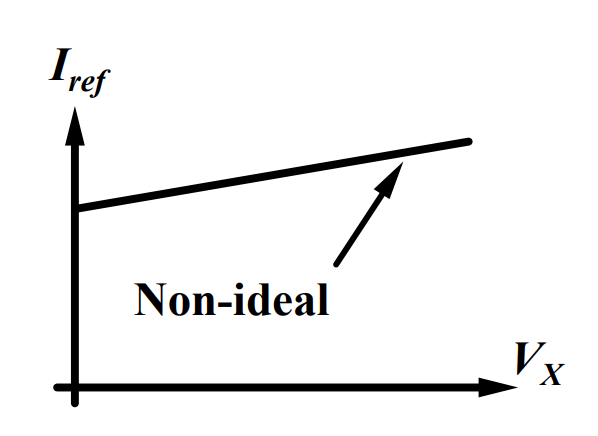
this slop will be horizontal if Rout is infinite
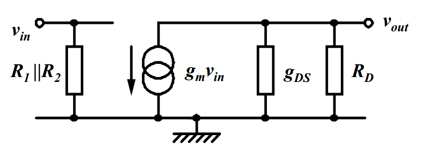

where gm is from transistor, and gds+GD is for other resistance
Diode connected FET
the Diode connected FET is always in saturation region, which can be seen as a resistance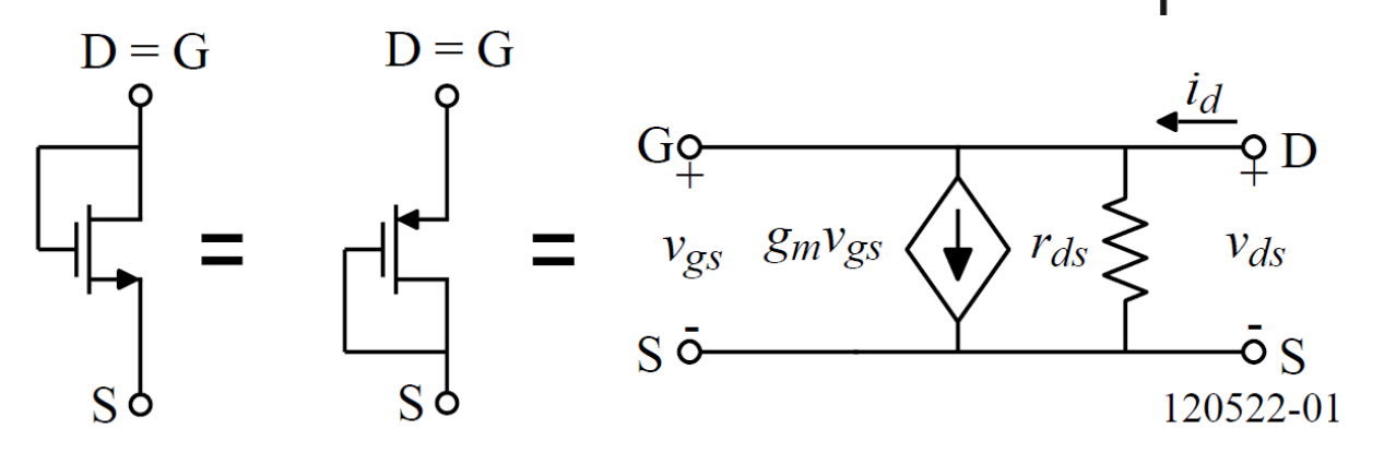

where VDS=VGS, AC resistence assumed as 1/gm
a Diode-connected active load is: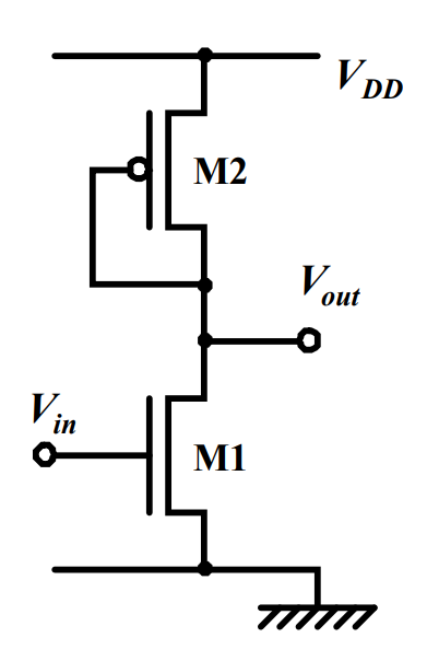
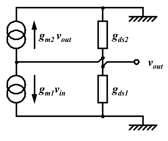
gm2Vout can be seen as a resistance g2. hence
because gm>>gds,
Av will just be like -gm1/gm2, and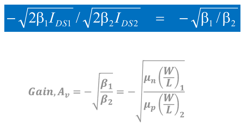
So the gain will be very small in this amplifier.
For high gain, then the device will have disproportionately wide or long transistors, which will cause limited bandwidth
Which channel length modulation: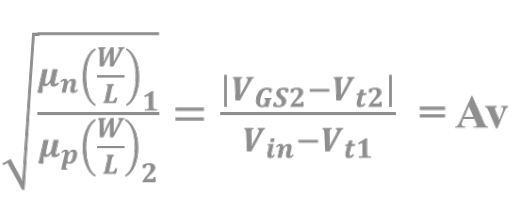
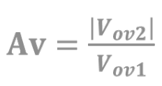
Key points:
Gain=gm*Rl
where gm converter input voltage to input current,
and Rl converter output current into output voltage
Bandwidth=1/(Rl*Cl)
where Rl is output impedance
Cl is output load capacitor
Hence Gain-Bandwidth product (GBP)=(gm * RL ) * [1/(RL CL )] = gm /CL
Current Source Load
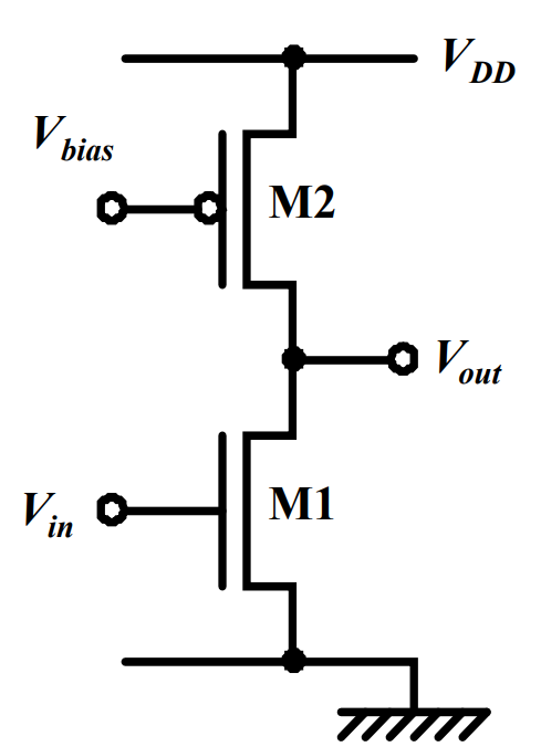
the P-mos can be seen as current source and must in saturation region
while N-mos is best be saturation
small signal: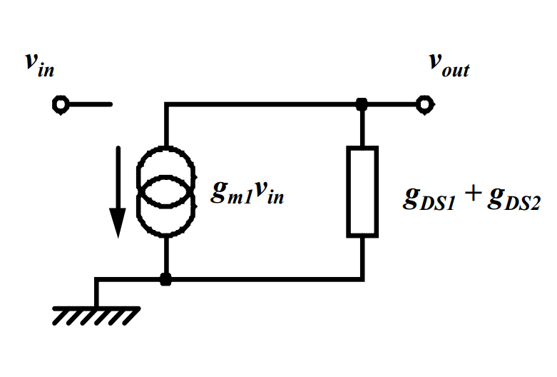

FET amplifiers (part2)
Two Transistor (CMOS) Amplifier
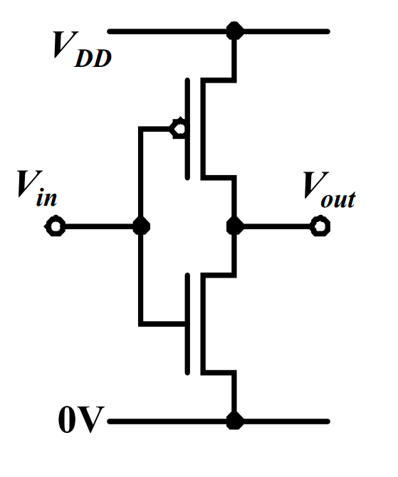
Advantage: high gain, not too many noise
Disadvantage: hard to maintain DC bias, take lot DC current
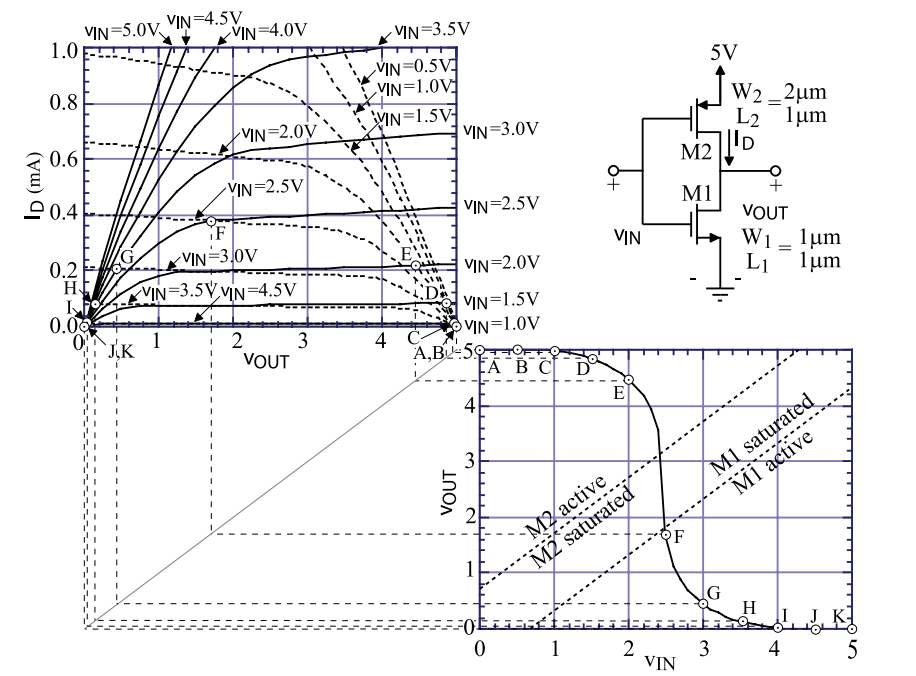
The current is maximum vakue if P-mos and N-mos are saturated
input voltage -> id current -> output voltage
N-mos: A->C cutoff, C->E active, E->F saturated, F->K active
Pmos: A->E Active, E->F Saturated, F->I Active, I->K cut-off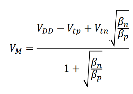
VM is voltage when Vin=Vout
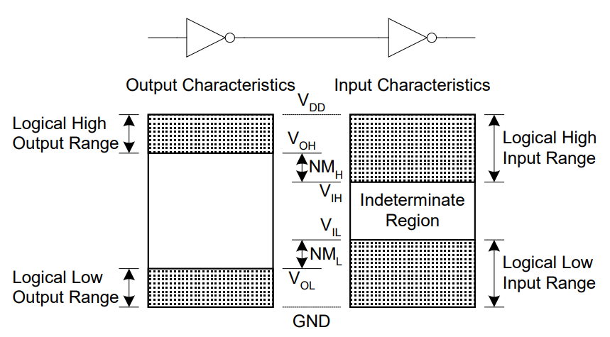
(?)
Note that in Cmos Amplifier, the T-rise time will be shorter than T_fall time, as resistance in P-mos is smaller than in N-mos
small signal analysis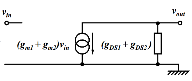

Source follower (common-drain circuit)
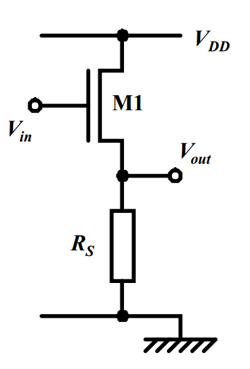
- use N-mos
- SF has gain approximate as 1
- Can be seen as a buffer
- Easy to have body effect as VBS=Vout is large


which gain will slightly less than 1
So SF usually beed connect bulk and source together to limite body effect, but also will limite bandwidth
Cascode amplifier
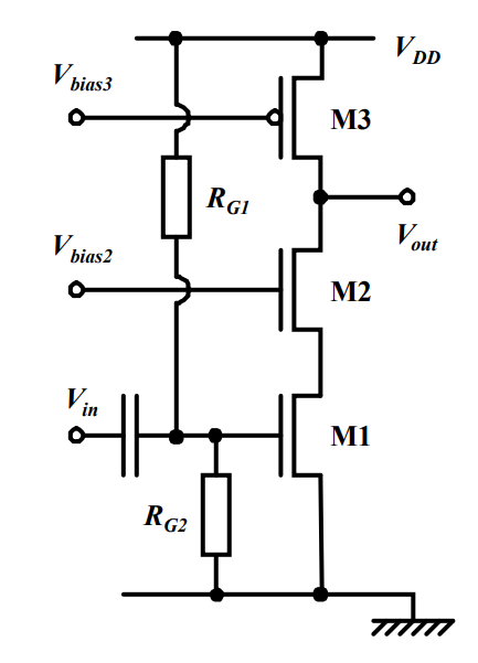
- R3 is a current-source load, and also can be seen as a resistance
- Vbias2 is constant, so VS2 is also constant
- So M1 has a constant current, and no λ term in M1. Hence output resistance of M1 is very high
- No Miller effect
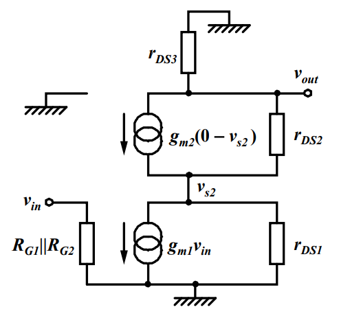
M3 has been a resistance

the amplifier with cascode can increase its gain in factor of gm2/gDS2
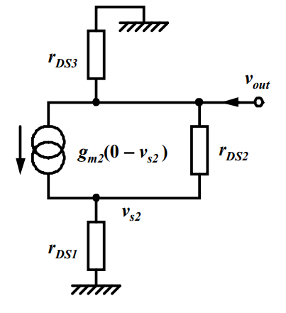
the Vin can be ignored because only output current is interested

output resistance is only related with M1 and M2
Hence Cascode can increase Gain and output resistance in factor of gm2/gDS2
AC circuit analysis
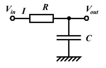
the RC circuit is a low-pass filter. It has circuit bandwidth: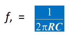

So the final bandwidth is completely controlled by resistance and capacitor: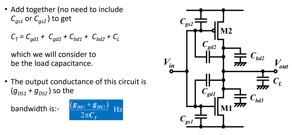
the small signal cna be chaned as: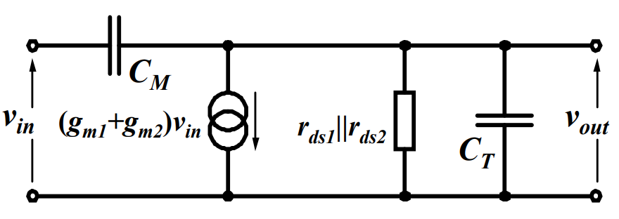
where CM = Cgd1 + Cgd2
according to node analysis, Rout can be changed as: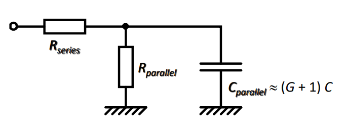
R_parallel ≈ Rin , just the original value
R_series ≈ Rout /(G + 1), relatively small
and the small signal can be changed as:

- two amplifiers are in cascade
- Cin1 and Cin2 will be increased greatly based on Miller effect
Body effect
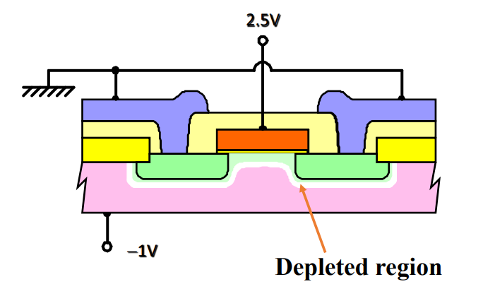
Normally the bulk is connect to VDD or VSS to svoid body effect,
But Change the voltahe drop on substract will influence threshold voltage.
- if bulk voltage drop decreased, more wider the depletion region will be
- wider depletion region need to charge more electrics
- Vt threshold voltage is related with depletion region’s charge effect
- So bigger body effect means bigger threshold voltage

φf is usually 0.35V, γ is usually 0.5(V)^(1/2)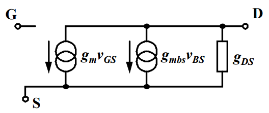
gmbs is based on body effect
Current mirror
Both n-type and p-type transister can be analyzed as current source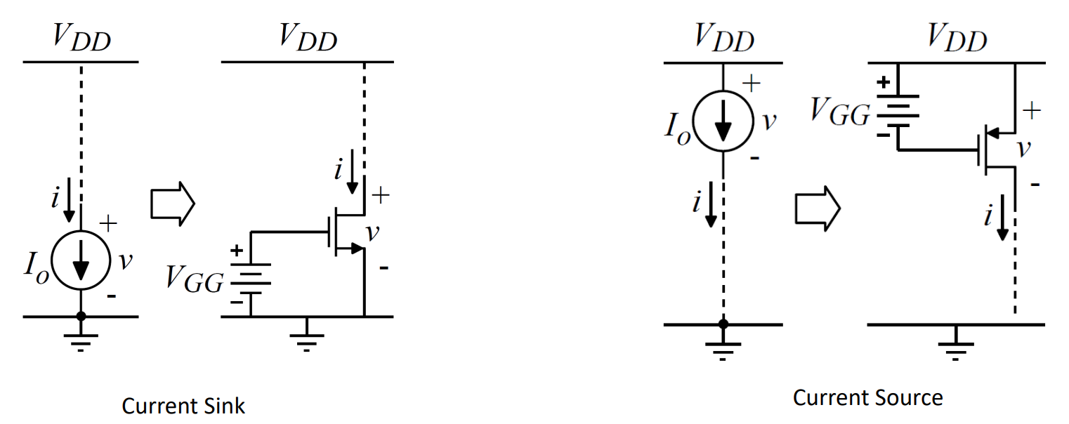
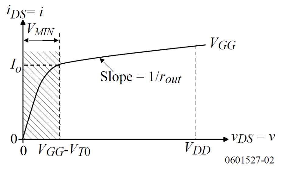
a ideal current source should have vary high output impedance and very low input impedance, means gain of amplifier will be really low -> only current, but no voltage, will be changed
Basic current mirror
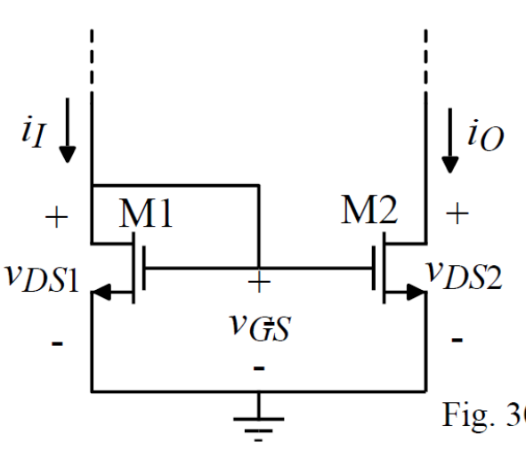
Rout=1/λId
Rin≈1/gm
If we assume:
Vmin(M1)=Von+Vt, than
Vmin(M2)=Von
hence both transistors must in saturation region
Small signal of M2: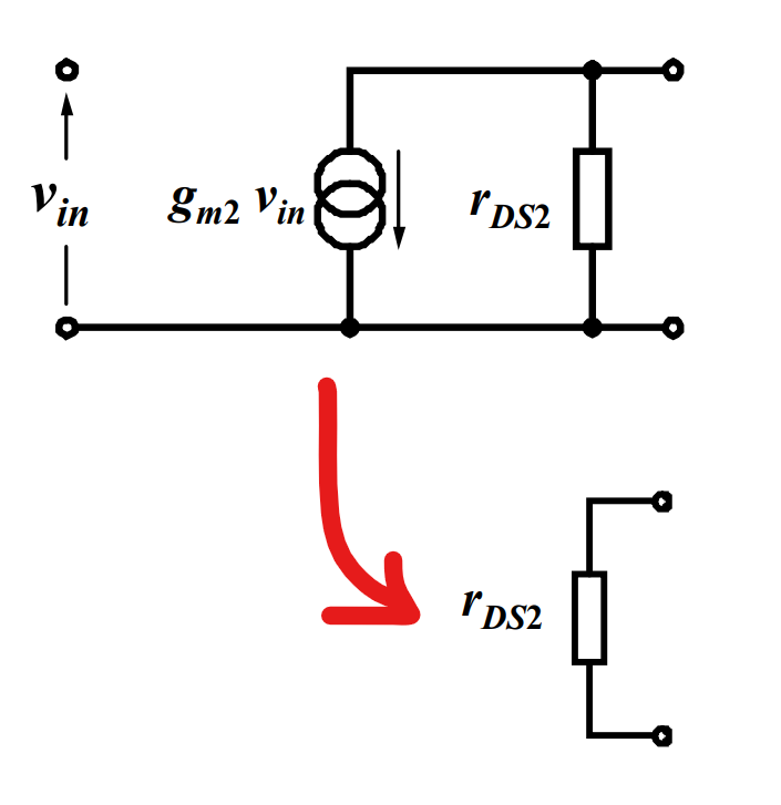
because vin from M1 is always constant, hence Vin is a DC voltage, hence should be ignored in this case
hence M2’s small signal circuit is just a resistance
Where rDS2 is rout
- fixed Iref and M1 makes VGS2 constant
- constant VGS2 and saturated M2 makes Ids2 constant
- But value of VDS2 is variable, so Ids2 will also varying
So we have a small input impedance and huge output impedance (1MΩ, but still not enough to most purpose)
Wilson current mirror
Wilson current mirror is a negative feedback system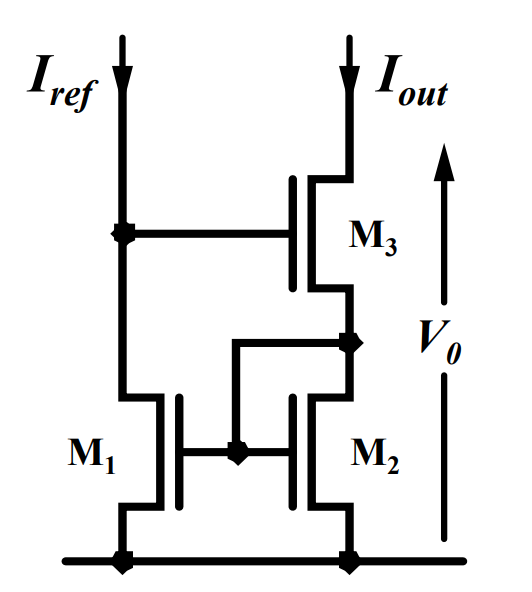
- if Iout rises, VDS2 also rises
- VGS1 rises, but Iref not change, hence VDS1 falls
- VGS3 falls, hence Iout falls again
current gain of Wilson current mirror is same as basic current mirror
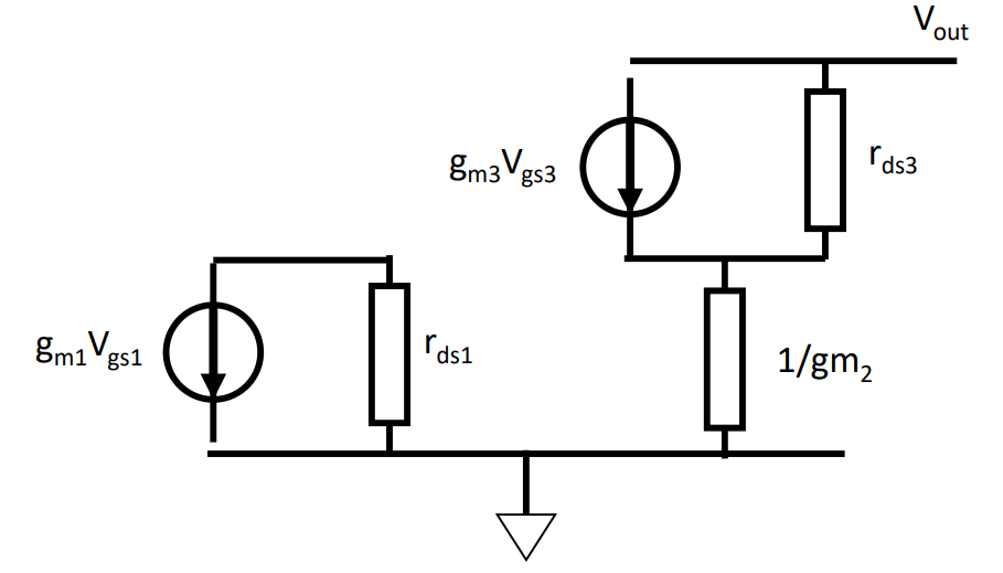


So rout≈gm*rds^2
Vout(min)=2Von+VT,
as VDS2=Von+VT, VDS3=Von
Cascode current mirror
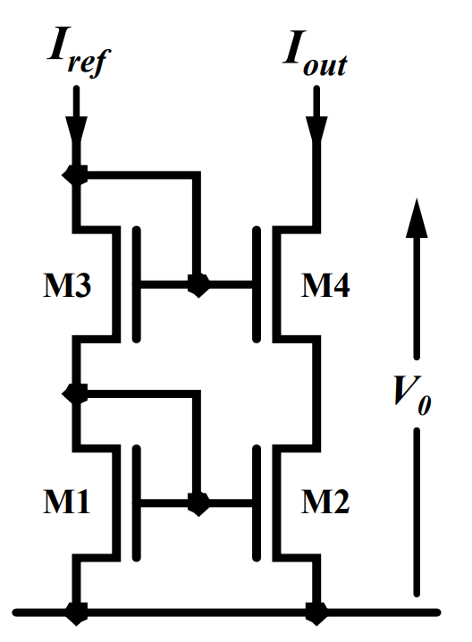
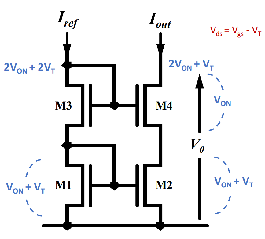
analysis order: M1 -> M3 -> M4 -> M2
Vout(min)=2Von+VT,
and VDS1=VDS2, which mean no need to worry about channel length modulation
small signal: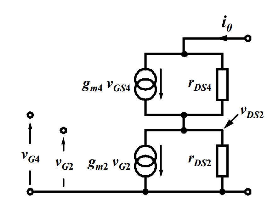
M1 and M3 are diode connect, can directly been ignored
VG2 and VG4 are all constant, hence VG2=VG4=0
hence VGS2=0, M2 just has resistance
1 | process: |
rout≈gm*ro^2
which is a hign output impedance
therefore,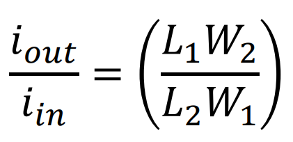
If we make W/L for M2 “n” times bigger than W/L for M1, Iout = nIref
This is an important result, as we could use it to make a DAC, as different W/L ratio will result in different current output, and we could sum them together to get analodge value.
Diff amplifier
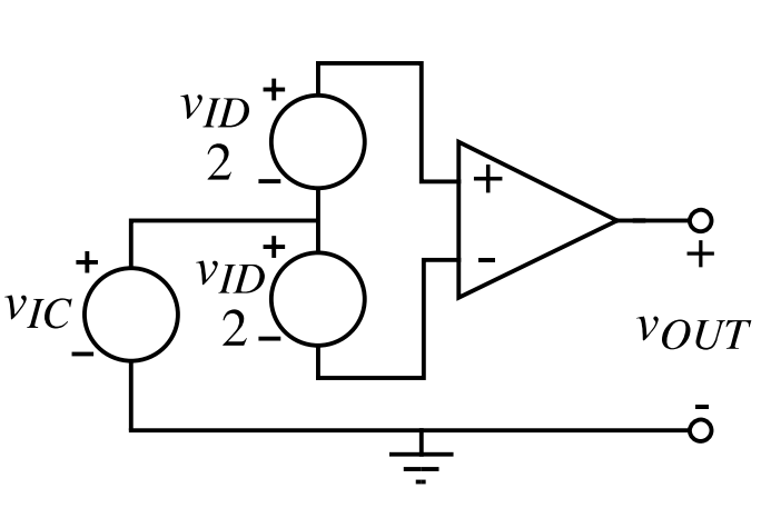
A differential signal: Measured between two nodes that have equal and opposite signal excursions around a fixed potential.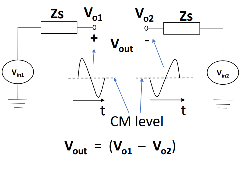
Note: the potential dash line in middle of borh signal is called ‘Common Mode’(CM) level
VP is VCM
Common-mode rejection ratio (CMRR):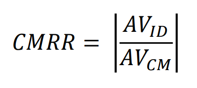
AVID = differential-mode voltage gain
AVCM = common-mode voltage gain
VID = differential-mode voltage (with different phase)
VIC = common-mode voltage
Large signal:
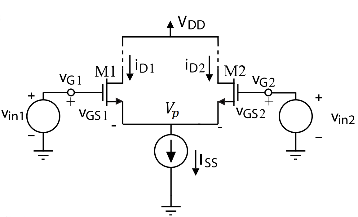
Vid=vgs1-vgs2
Iss=iD1+iD2
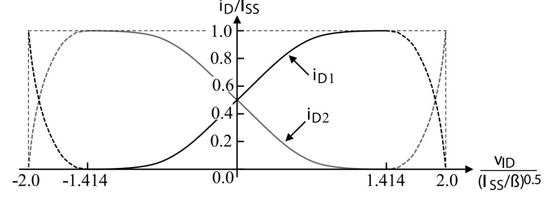
because ISS is from current source, it cannot change. Hence iD1+iD2 is always constant
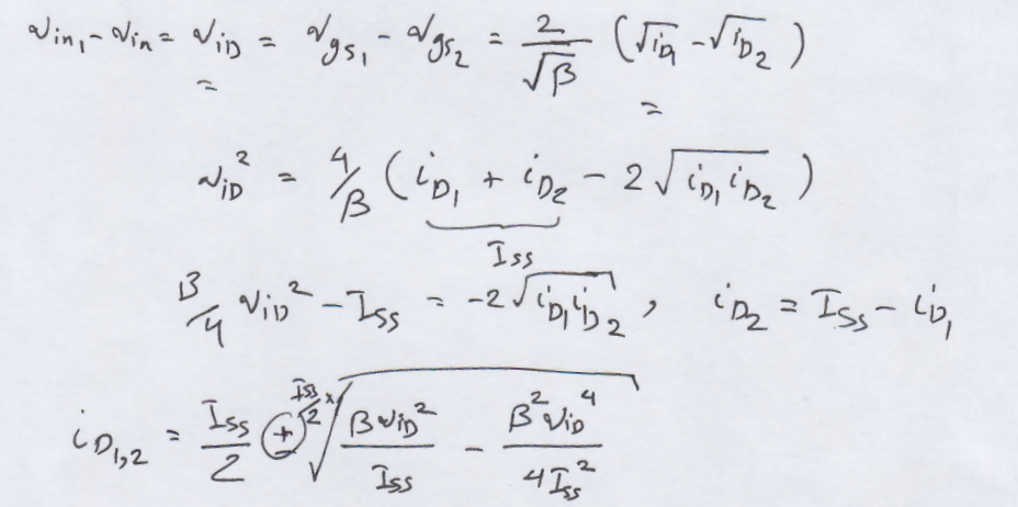

for differential gain: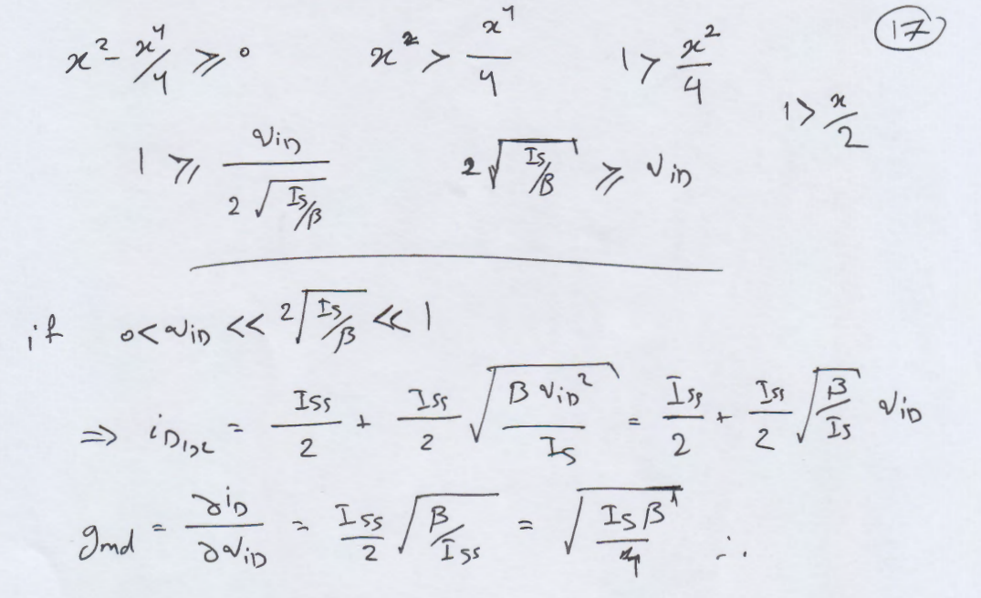
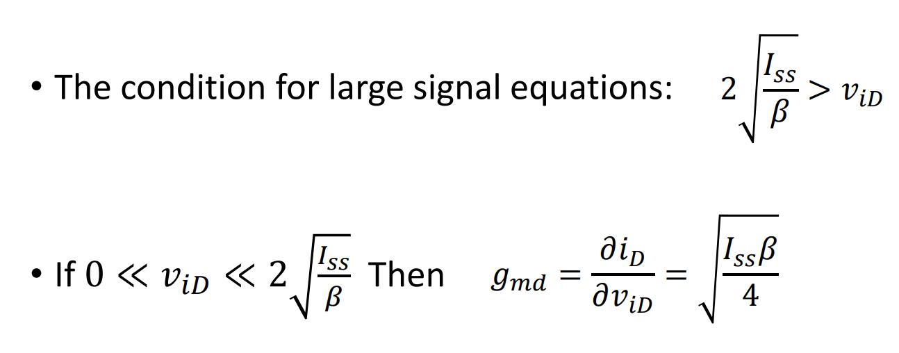
for common mode gain: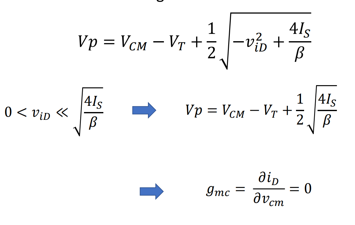
so iD and vcm have no relations.
Small signal:
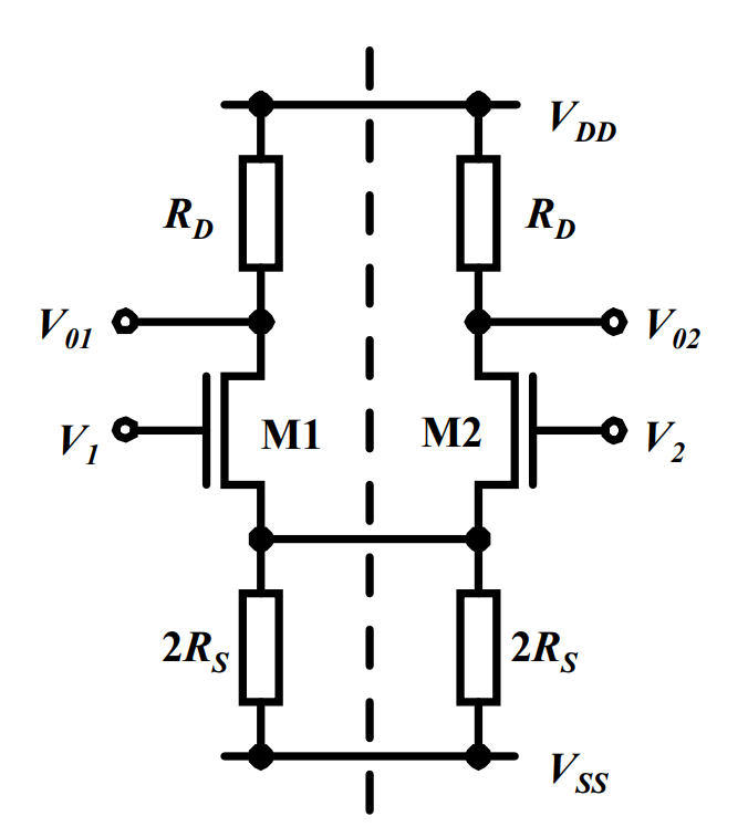
Small signal can only analysis half part because symmetric
parallel 2*2RS is total in RS only, the output impedence in current source

(?)
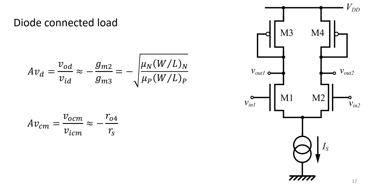
Diode connect load
Current mirror load
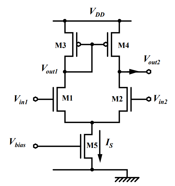
• Vin1 and Vin2 are VCM only
• gm1 = gm2
• gm3 = gm4
• ro1 = ro2
• ro3 = ro4
• I3=I4
Common mode: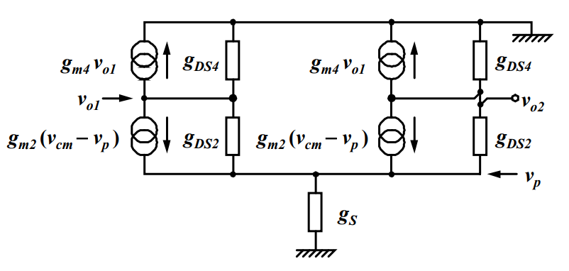
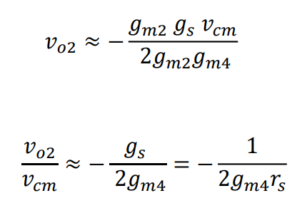
differential: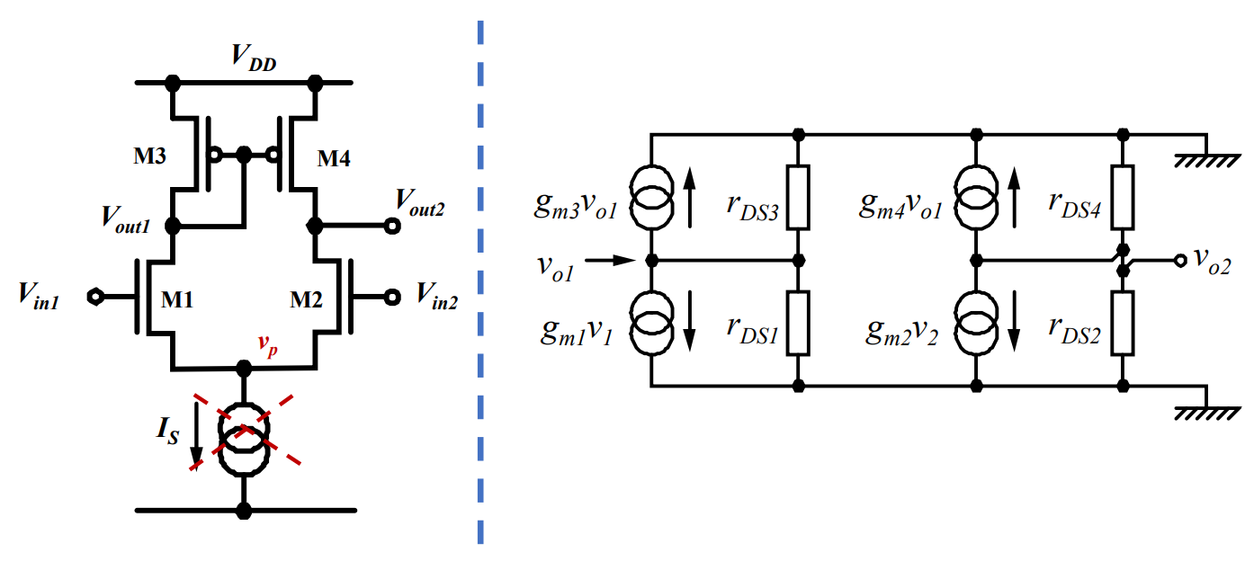
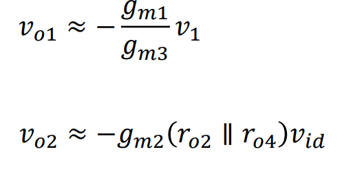
only o2 is related with differential voltage
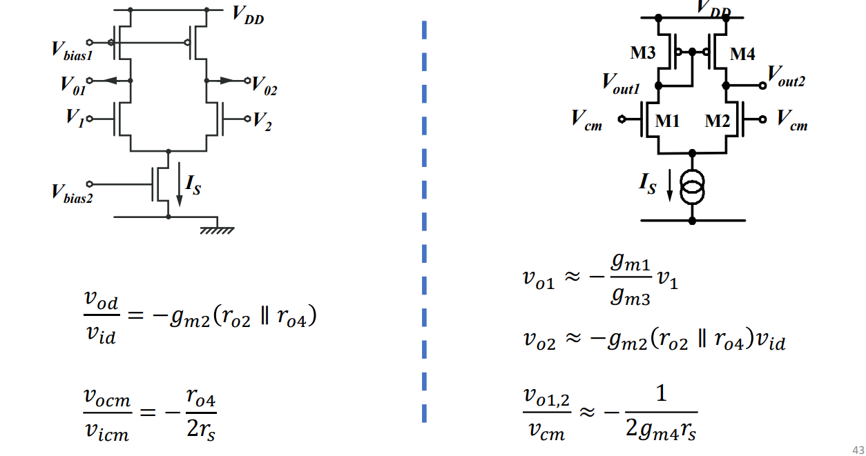
the current mirror amplifier is better,
as it has almost fixed common mode gain (around 1/2)
as big differential gain