Principle of Microelectronics
Formular sheets and slids: (https://pipirima.top/2022-2023/Principle-of-Microelectronics-Slides-4dd36568acfc/)
1-1
Blackbody radiation
Blackbody radiation is the thermal electromagnetic radiation within or emanating from a body in thermodynamic equilibrium with its environment, or emitted by a black body (an idealized physical body that absorbs all incident electromagnetic radiation) with a temperature above absolute zero.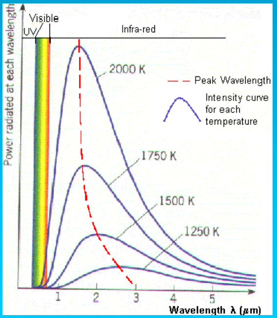
The higher the temperature of the body, the shorter the wavelength of the peak of the spectrum, and the higher the intensity of the radiation. the peak wavelength is in range of infra-red
Photoelectric effect
A physical phenomenon in which electrons are emitted from the surface of a metal or other material when it is exposed to light or other electromagnetic radiation.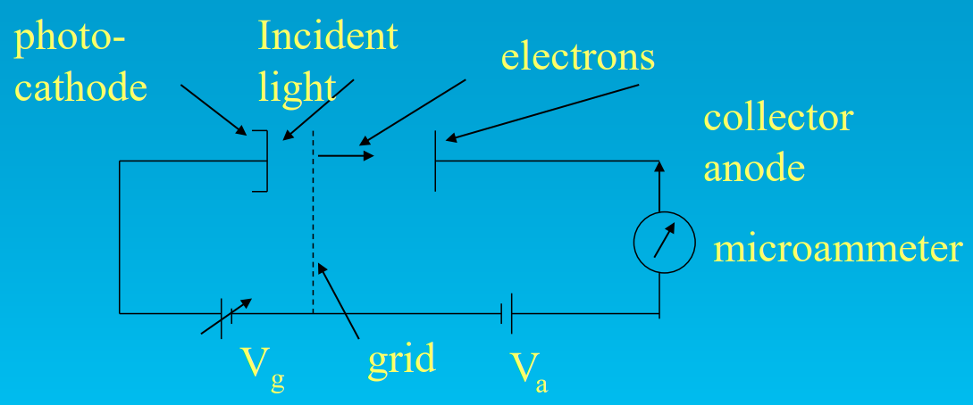
- Cathode part metal contact light
- electrons absorb energy in one photon
- if energy permitted, it will emitted to anode material
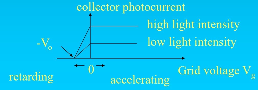
the electron has a constant energy required freuqnecy f0. if incident light freuqnecy f>f0, energy from photon is bigger than required energy level in electron, hence electron can be emitted.
the ourput current will be constant with stable light luminance. as one electron can only absorbe energy from one photon. the total current is fixed
the energy which allowed an electron just been emitted is called work function = eϕ, where ϕ is in voltage
the total kinetic energy an electron has when it is just been emitted is = photon energy – work function:
Bohr atom
Bohr atom is the atom with central nucleus with electrons travelling in a circular orbit around it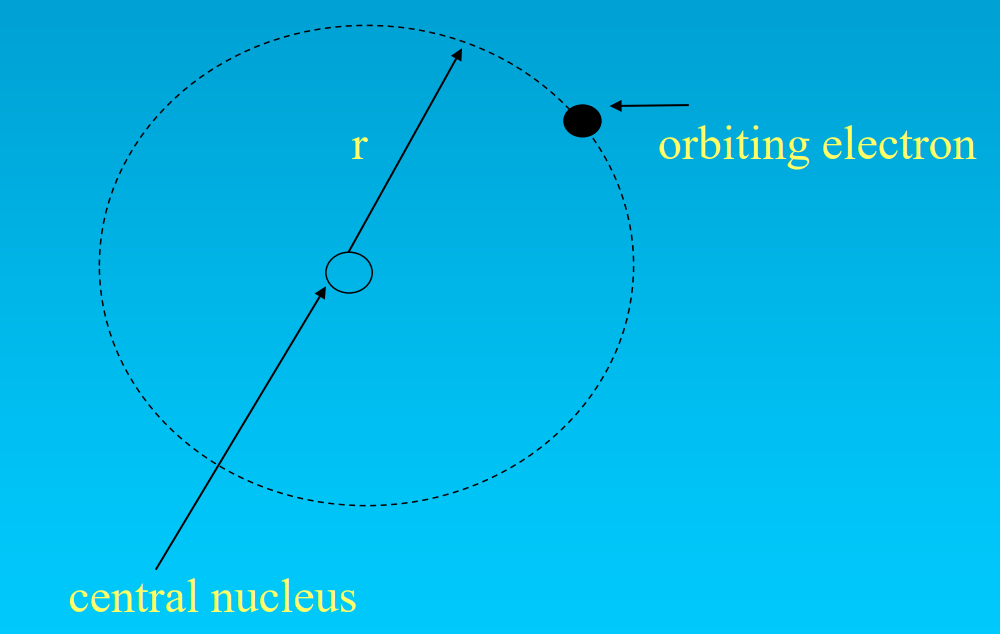
coulomb force on the electron due to the e-field of the positive nucleus is just sufficient to provide inward acceleration for circular motion at a constant radius r
the electrons can only allowed to make a transition from one energy level to another level.
Particle-wave duality

The momentum of the photons is:
where p is momentum in kg.m/s, h is constant, λ is wavelength
a particle can both conatins wave and particle properties
wave-packet
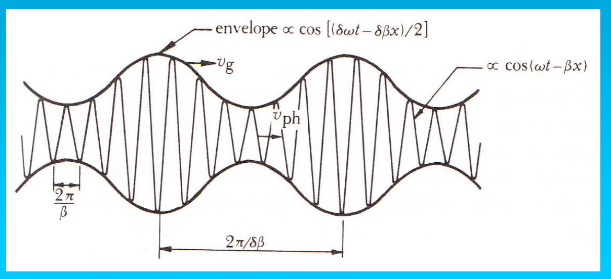
Wave-packets are useful for describing the behavior of particles because they allow us to describe the probability of finding a particle at a specific location at a specific time.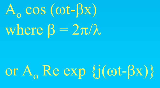
β=2*pi/λ
vph=vλ
vph is phase velocity, that represents the velocity of phases along propagation direction of the wave (small signal shape)
it describes frequency and wavelength of the signal
vph is possible to faster than light

group velocity is the shape of wave-packet (whole big shape). group velocity is usually less or euqal to phase velocity
Schroedinger equation
1D Schroedinger equation
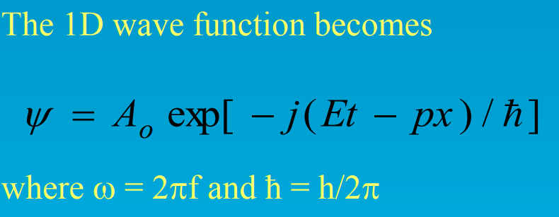

this equation governs the behaviour in 1D of all particles, but no proof method
3D equation

this equation can be simplifier by remove time-position dependent part: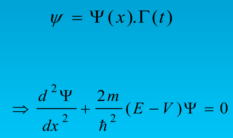
where Ψ is a function of space and time coordinates. it is one particle’s position in fixed time T.
Ψ is usually a complex number
and |Ψ|^2 ΔV is proportional to the
probability that a particle will be found in the volume element ΔV
like for the probaibility to find a particle in range x+dx,y+dy,z+dz:
Normalization
From previous function, it is clear that:
please note Ψ must in continious
Uncertainty principle
the accurate position and energy value can not be measured in same time.
this is mainly beacuse un-accurated measure methode. the measurment from one parameter will influence measurement to another parameter.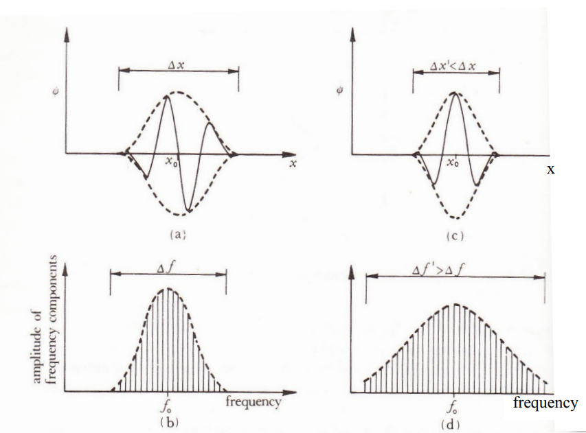
the accurency of x increase range of f
(?)
particles in potential box
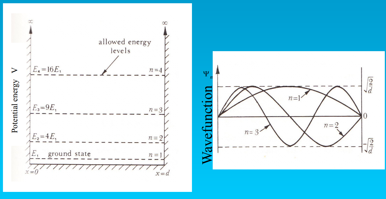
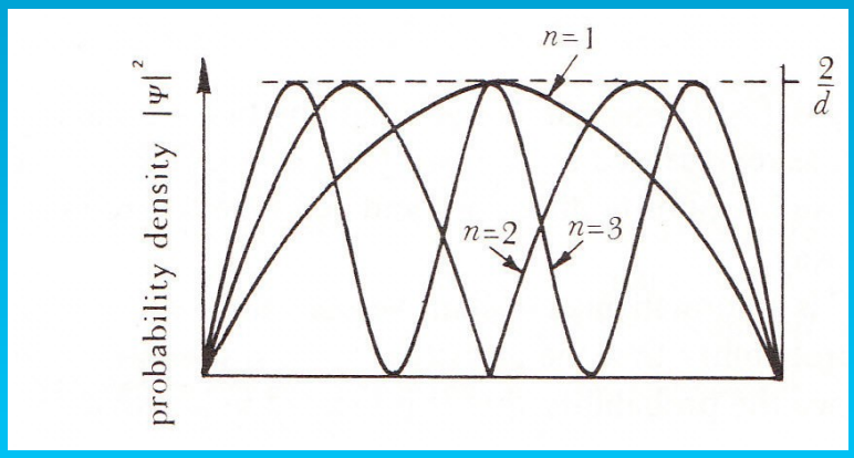
second plot is the probability where the particle is, when x axis is range form [0,d]. the sum of this wave may be the constant vlaue 1.
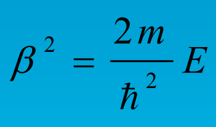

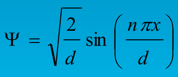
it can be simplified as: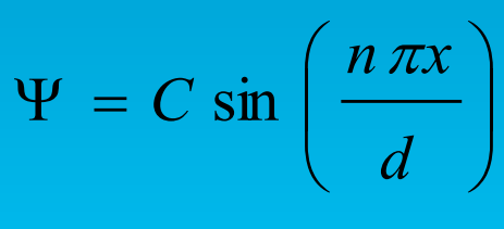

The total energy of the bound particle has only a discrete set of allowed values: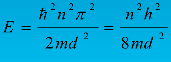
from page 31
(?)
Band gap
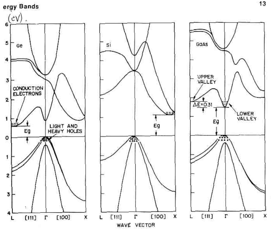

1D idealised model of an array of atoms in a solid Kronig-Penney model (square potentials)
the level of potential energy can be seen as probability of electrons
if 0 <= x <= b, V=0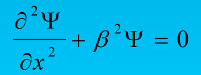

if x>b, V>E,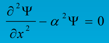
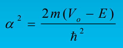
Now if the w becomes vary small and L becomes infinity, wV will be constant, and equation changes as:
Uk is the Bloch function, a periodic function which varies with the same periodicity as the S equation is in periodically
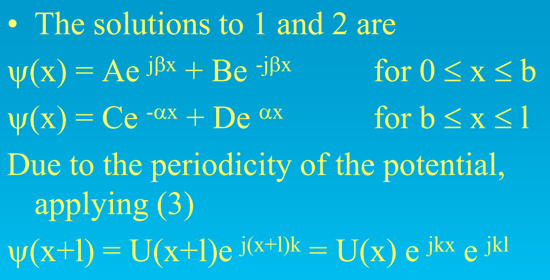
and note E=h^2/2m^2, where E is free electron case. the electrons can move freely in solid
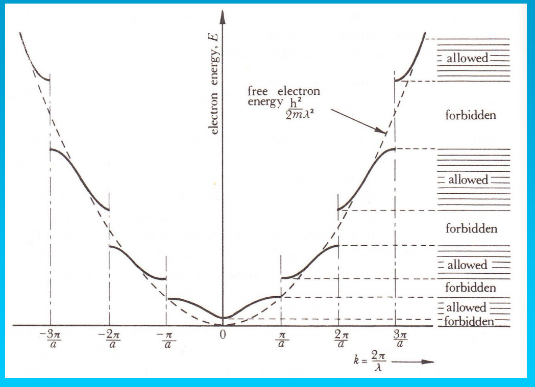
x-axis is momentum
this figure shows all possible position that electrons will be
hence, energy gap will appeared between soild material
it will be influenced by electric field,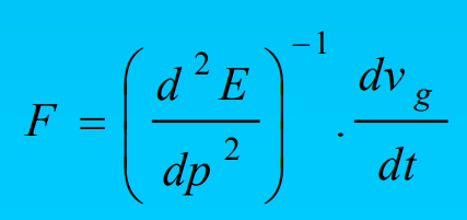
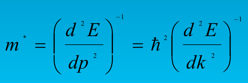
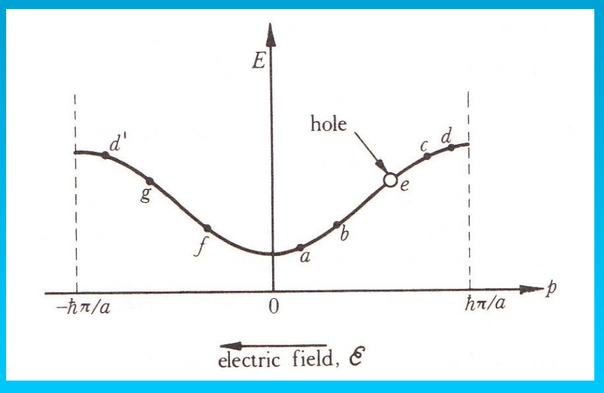
from a -> b, energy increased, velocity is also increase
from c -> d, energy increased, velocity is decreased (trend <1)
from page 29 (?)
Metal-semiconductor contacts
When contact is made between two dissimilar materials, a contact potential (barrier) typically develops at the interface between the materials
can be categorised as non-rectifying (ohmic) and rectifying (Schottky barrier type diodes)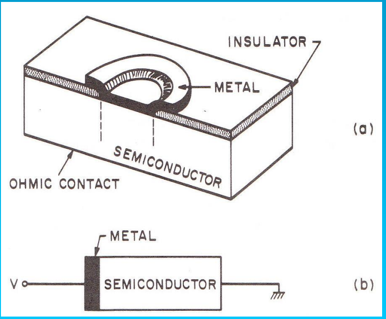
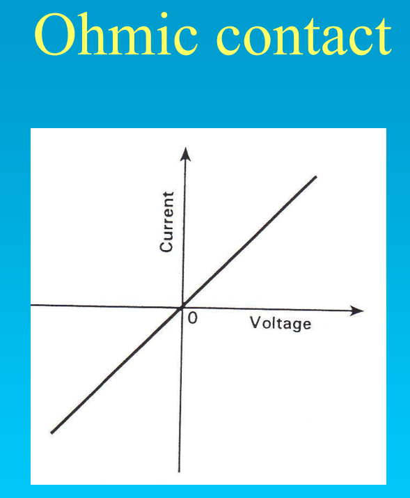
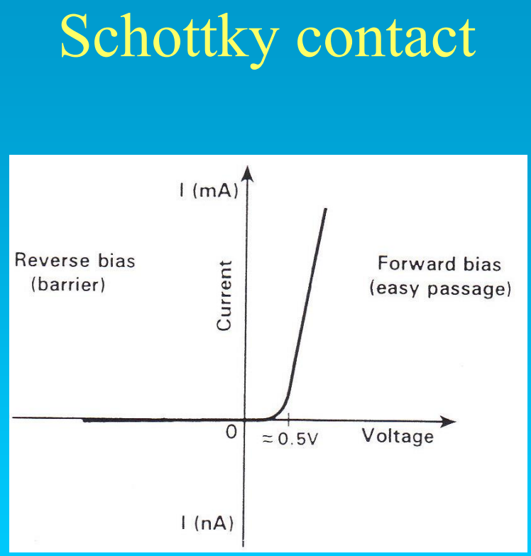
contact: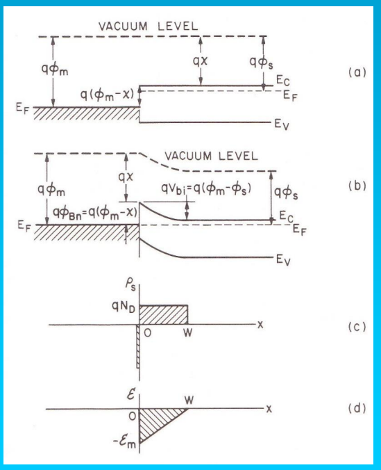
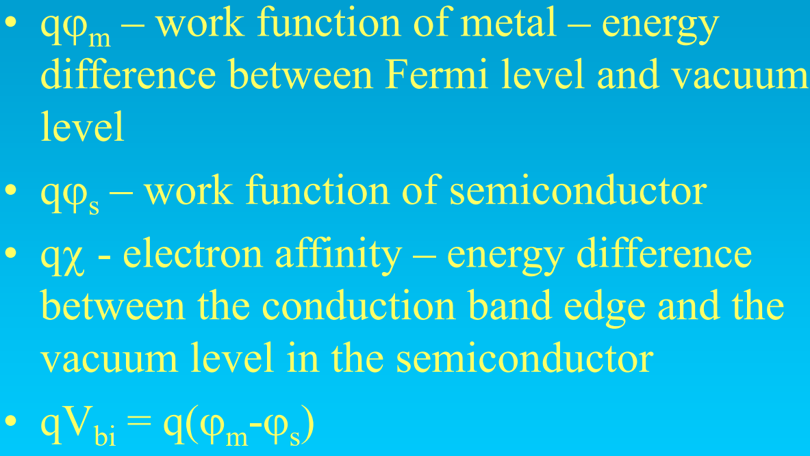
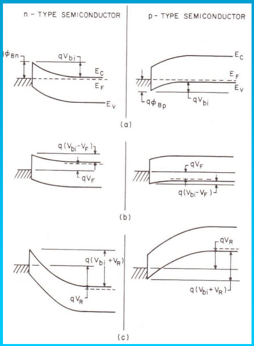
Ohmic contact:
allows current to flow in either direction with contact resistance as low as possible (no barrier)
if Ψm<Ψs: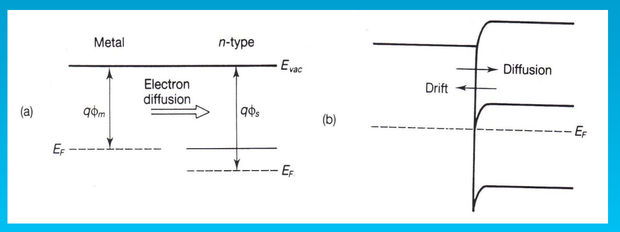
celectrons with no bias
and because majority is electrons (n-type), hence this is ohmic contact
but if Ψm>Ψs:
the specific contact resistance Rc depends on doping
high doping it has, more narrow the barrier will be
the contact resistance depends on:
- metal and semiconductor work functions
- temperature
- chemical reaction
Schottky contact:
only allows current to flow in one direction
must be Ψm>Ψs
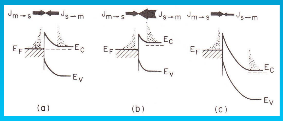
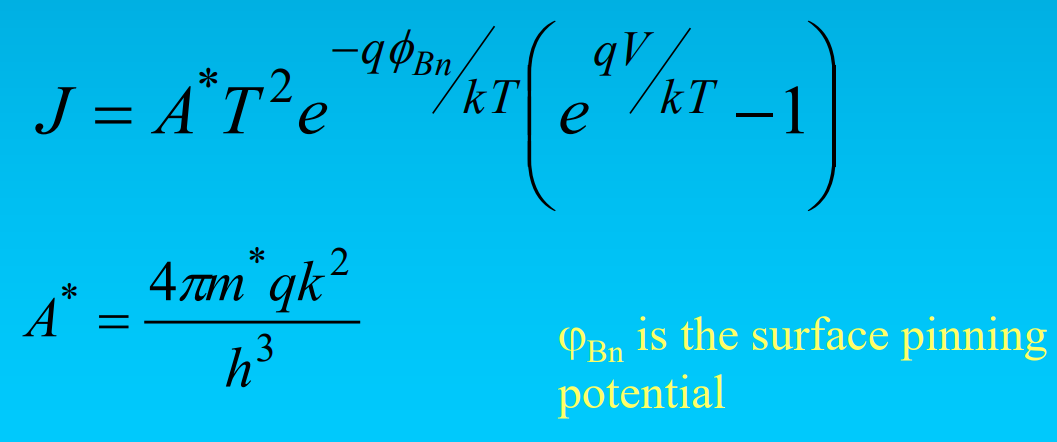
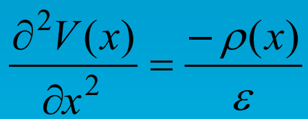
The relationship between charge and potential in a Schottky diode is from Poisson’s equation:
V is the potential, ρ is the charge density, ε is the permittivity and r is the real space vector
The total charge is:
where A is the diode area on the semiconductor surface
Anderson’s rule
the vacuum levels of the two materials of a heterojunction should be lined up
∆Ec=Ec_B – Ec_A = χA - χ B
χ = electron affinity of the material, which is independente with Fermi level
e.g. GaAs has χ = 4.07eV and Al0.3Ga0.7 As has χ = 3.74eV, predicting ∆Ec = 0.33eV
Heterjunction
A junction between p-type and n-type layers in the same material is called a homojunction
A junction between two different materials is called a heterojunction. they offer to manipulate the behaviour of electrons and holes through band engineering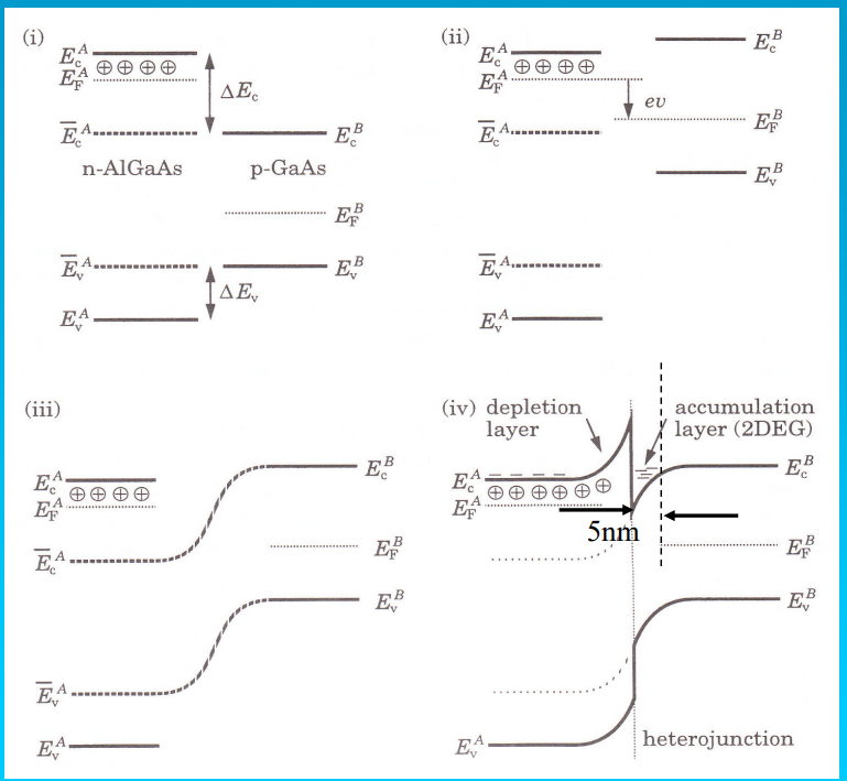
High Electron Mobility Transistors (HEMT):
Main reasons for their superior behaviour
Modulation doping:
- High mobility due to reduced scattering as partocles are all stopped in carrier channel
- Can control gain by optimising carrier density, space layer thickness, channel distance
- Can choose material with a small effective mass (hign intrinsic carrier mobility)
The maximum transconductance increases, as
- increasing threshold voltage
- increasing doping of the AlGaAs layer
- decreasing space thickness
By making T-shaped gates – decreases the RC time constant for switching
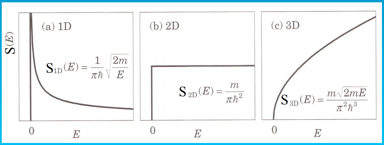
Density of state
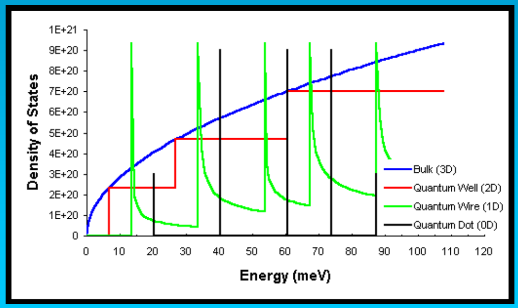
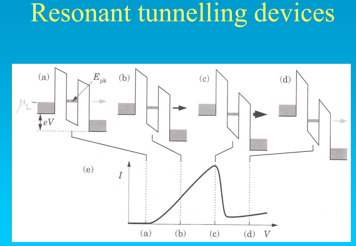
High current appear if Epk is horizontally matched with grey area in left
Hall effect
If a current is passed through a semiconductor and a magnetic field B is applied at right angles to the direction of current flow, an electric field is induced in a direction mutually perpendicular to B and the direction of current flow.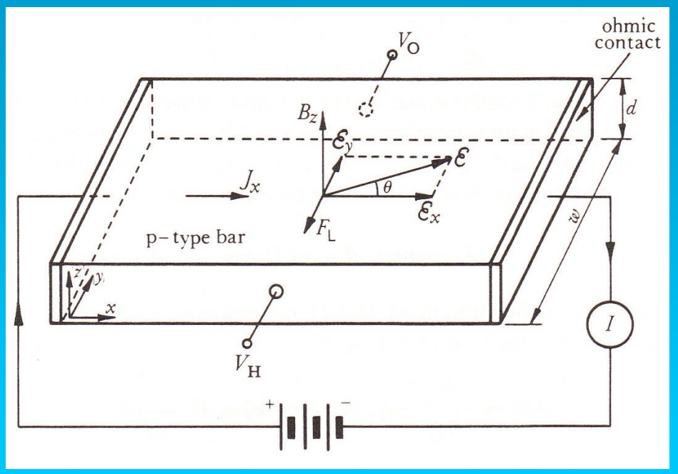
The Hall coefficient, RH: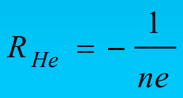
Hall mobility:
Hall bar structure: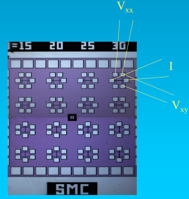
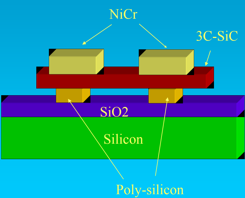
advantages:
- can combine etching and releasing together
- suit for batch process
- can be designed during MEMS design
Liquid crystal display (LCD)
EMR:
Visible light is a form of Electro-Magnetic Radiation (EMR) with wavelength in the region 390 - 750 nm (790 - 400 THz).
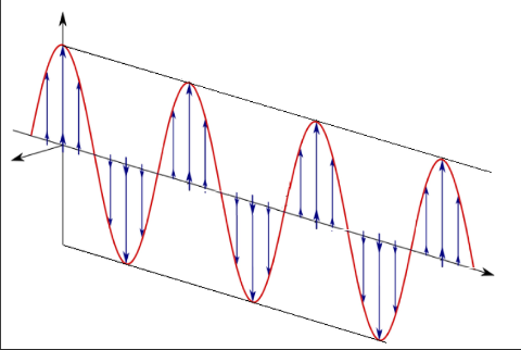
EMR have both electric and magnetic field components. the normal propagating traced as an ellips, but some special cases will include a circle (circularly polarized) or a straight line (linearly polarized)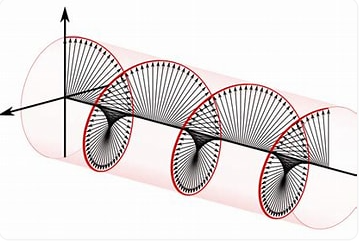
liquid crystal
“liquid crystal” describes a group of meso-phases between solid crystal and isotropic liquid that exist for a number of organic molecular materials.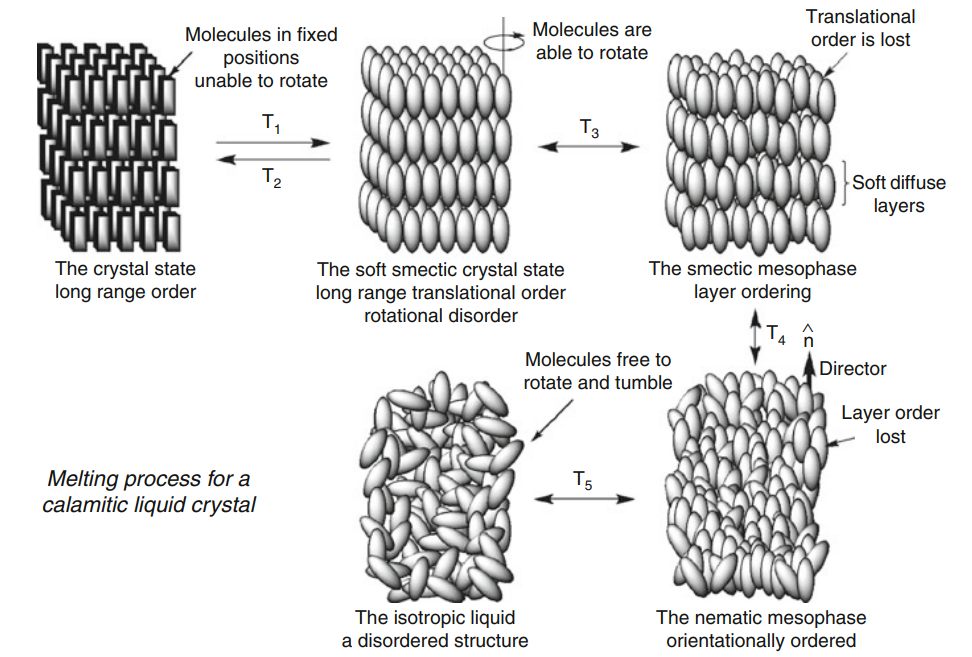
liquid crystal is a state between liquid and solid. It can bound some moleculars, but can also rotate.
the LC moleculars are normally in two shaps: rod-like (used in LCD) and disk-like (in other applications)
The LC particles can usually be aligned by some ‘surface force’ when placing between two plates. We can also control their direction by electric field.Use electric force.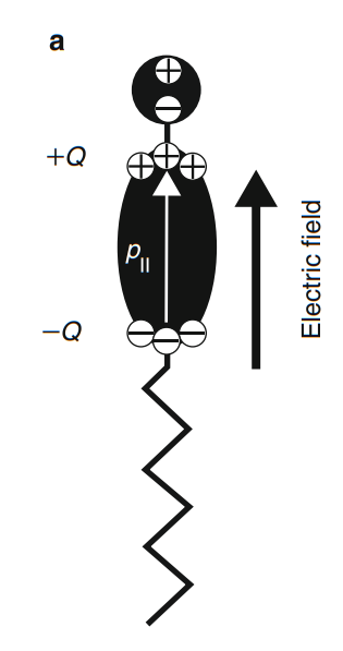
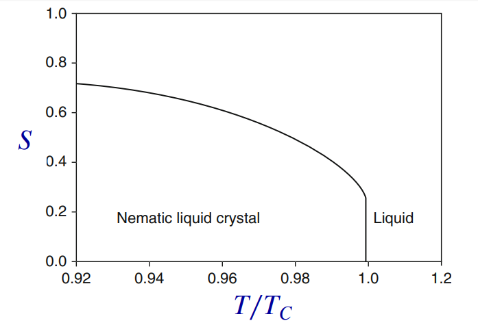

S is an order parameter that shows how well the eceltric field control LC’s direction. bigger S is, more LC moleculars will face the correct direction
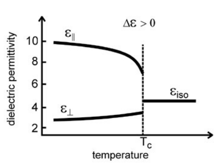
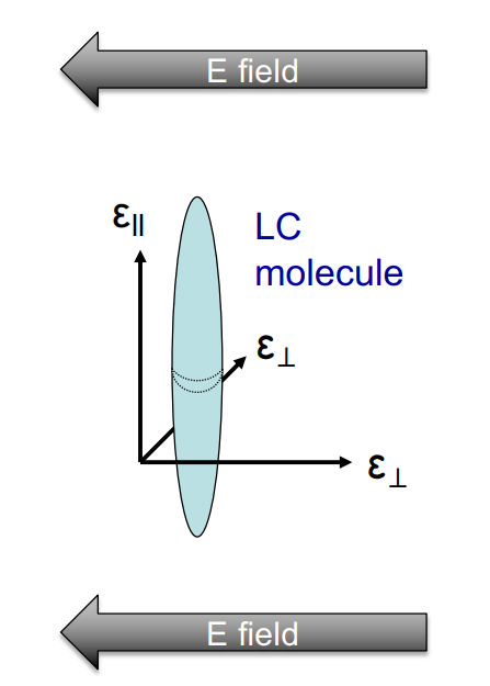
the dielectric permittivity ε is a physical quantity describes how LC molecular will be effected by electric filed.
dielectric anisotropy is: Δε = εII - ε⊥
if Δε>0, LC molecular will be parallel with electric field,
if Δε<0, it will be perpendicular with electric field.
many LC material configurations exhibit switchable birefringence, where birefringence material is one in which the refractive index alongone axis (extra-ordinary) is different to that along the other two (ordinary) perpendicular axesl that outputs two different polarized light waves, like rambow-colored plastic.
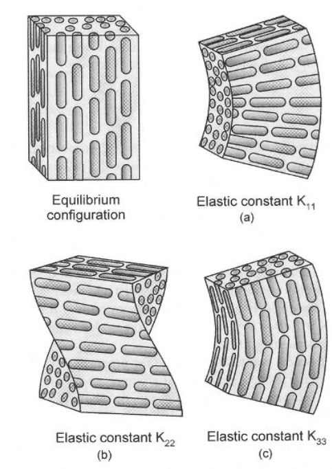
(a)Splay shape, k11
(b)Twist shape, k22
(c) Bend shape, k33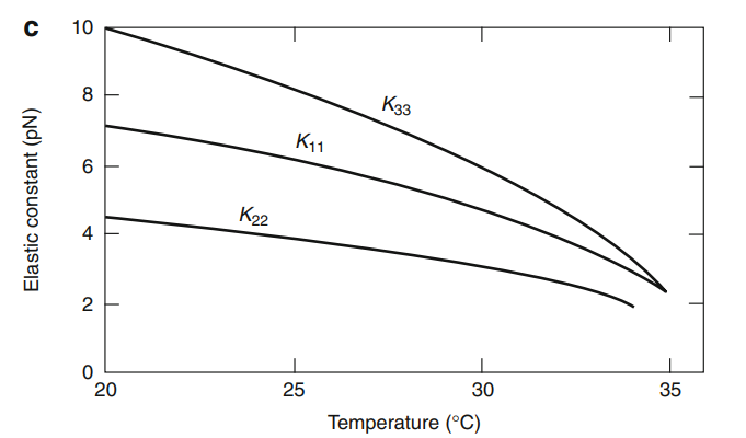
this is a basic LCD structure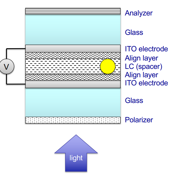
- Analyzer and Polarizer are all polarized board.
- Indium Tin Oxide (ITO) electrode is a transparent conductive material,
- Align layer can align LC particles into twisted or other shapes whenthere have no electric field
- LC layer <1 to several µm thick
- Modern LCD has many other structures
Twisted Nematic (TN) Effect
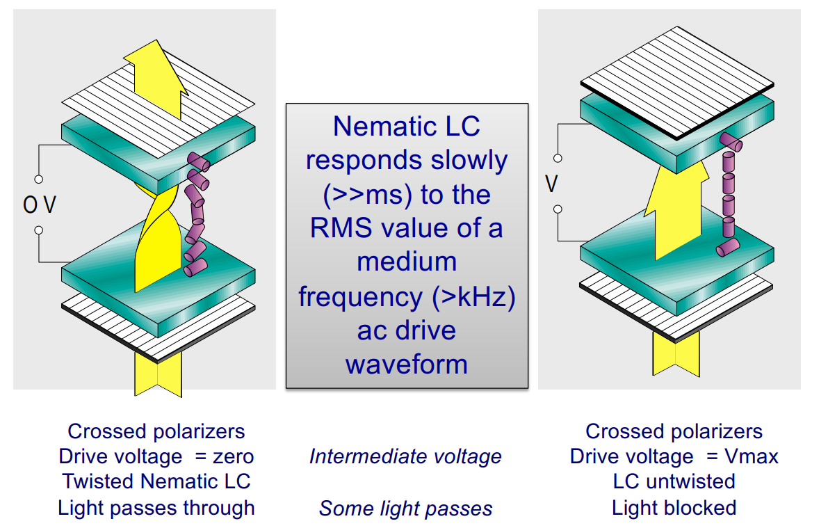
left part can pass the light, but right part will block the light.
the twisted LC psrticles are influenced by align layer, while straight LC particles are forced by electric field
the Active-matrix liquid-crystal display (AMLCD) strcture: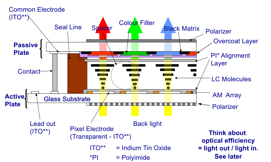
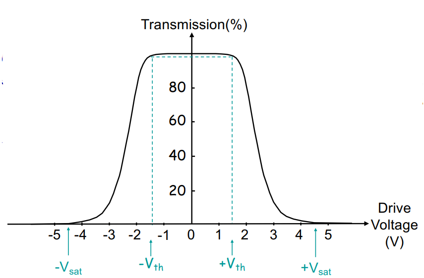
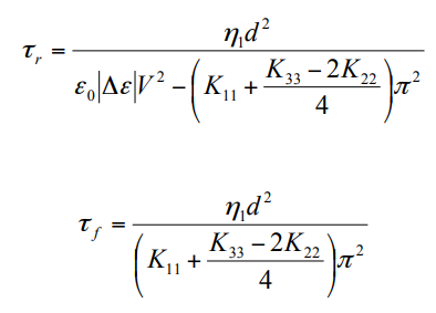
Vth is the point when LC particles start to move based on electric field, which is called Freedericksz Transition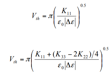
Vertically Aligned (VA) LC
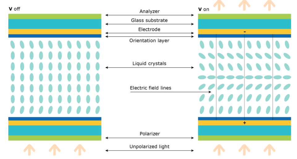
VALCD use negative dielectric anisotropy which are aligned perpendicular to the electric field
In-Plane Switching (IPS) LC
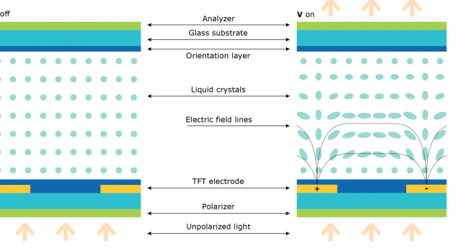
use positive dielectric anisotropy, and creates much lower viewing angle dependence than in TN and VA displays
LCD passive matrix addressing
LCD can be drived by active-matrix driver or passitive-matrix driver.
we want fast in active matrix, but slow in passitive matrix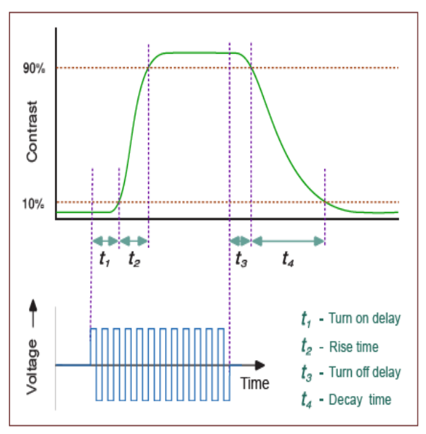
the passive matrix: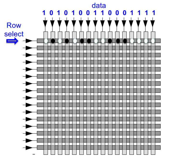
• Back electrode is vertical columns
• Front electrode is horizontal rows (?)
• M*N pixels requires only M+N drivers
working process:
- select first row
- drive some column lines, so some pixcels on first row will turn on
- select seond rwo, and go on
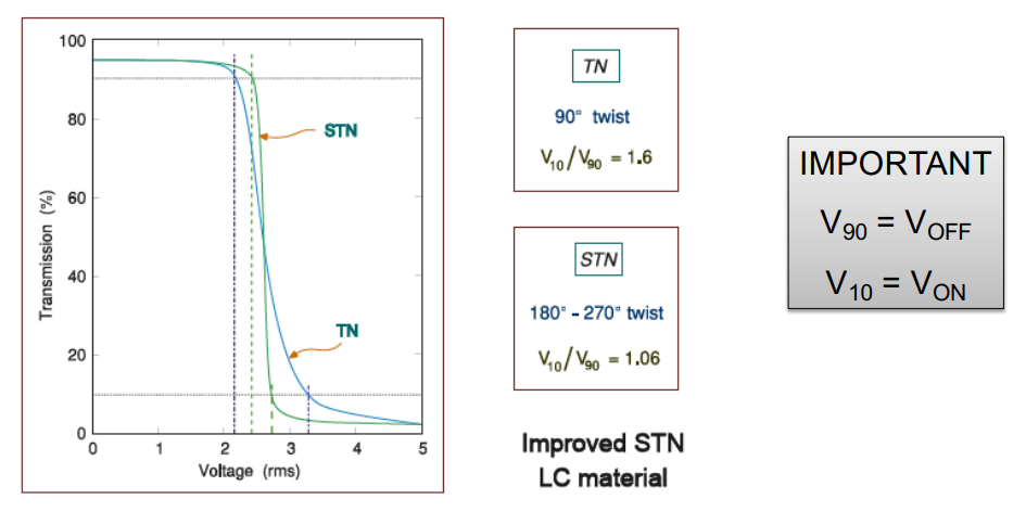
the real waveform of passive matrix, assume Vth=1.7V, is like: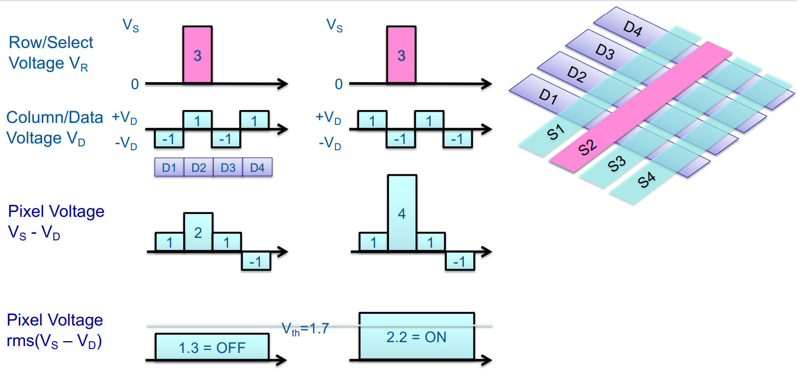
where 3-1=2, Voff=((2^2+3)/4)^0.5=1.3
3-(-1)=4, Von=((4^2+3)/4)^0.5=2.2
foe example, in following figure, only point D2S2, D2S3 will turn on
S1,2,3,4 are turned one by one,
but D1234 are turned (on or off) in same time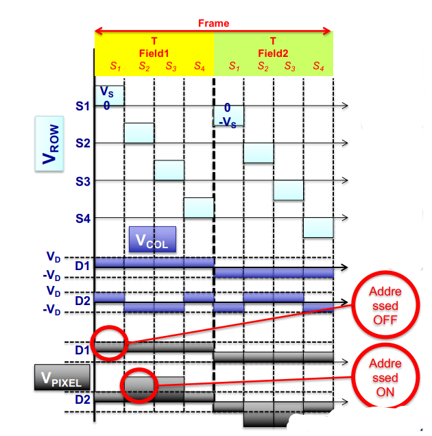
discrimination ratio: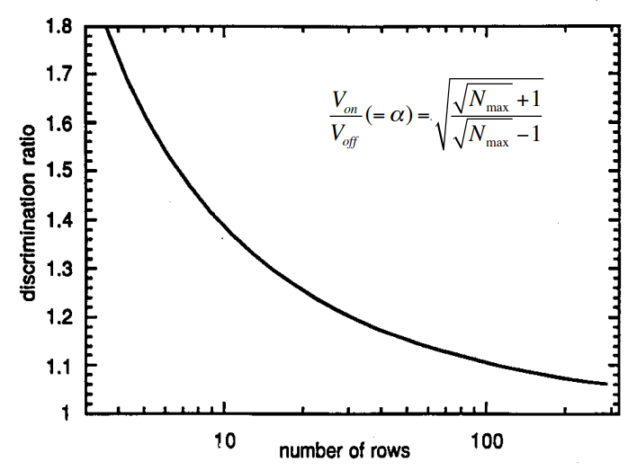
this will decrease rapidly with increasing number of rows N
in inverse, maximum number N ca be computed as: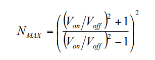
smaller Von/Voff has, more number N can be contained in design
| advantage | disadvantage | |
|---|---|---|
| passive-matrix | more lines than segmented | lines limited by design |
| cost↓ | when lines ↑, Limited contrast, pixcel Crosstalk, More driver requirements, more requirements for LC material |
LCD active matrix
the active matrix can:
- increase duty cycle
- reduce cross-talk
- simplify addressing waveform
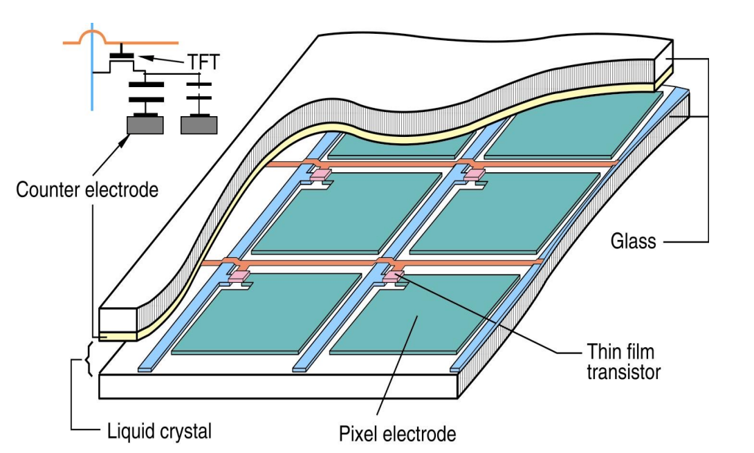
each group is combined with 1 TFT transistor, and 1 storage cup (pixcel electrods)
Other driver process is same with passive-matrix
- sweep column lines, and select row lines
- if pixel is selected, TFT will turn on
- storage cup charged
- liquid cyrstal open
row: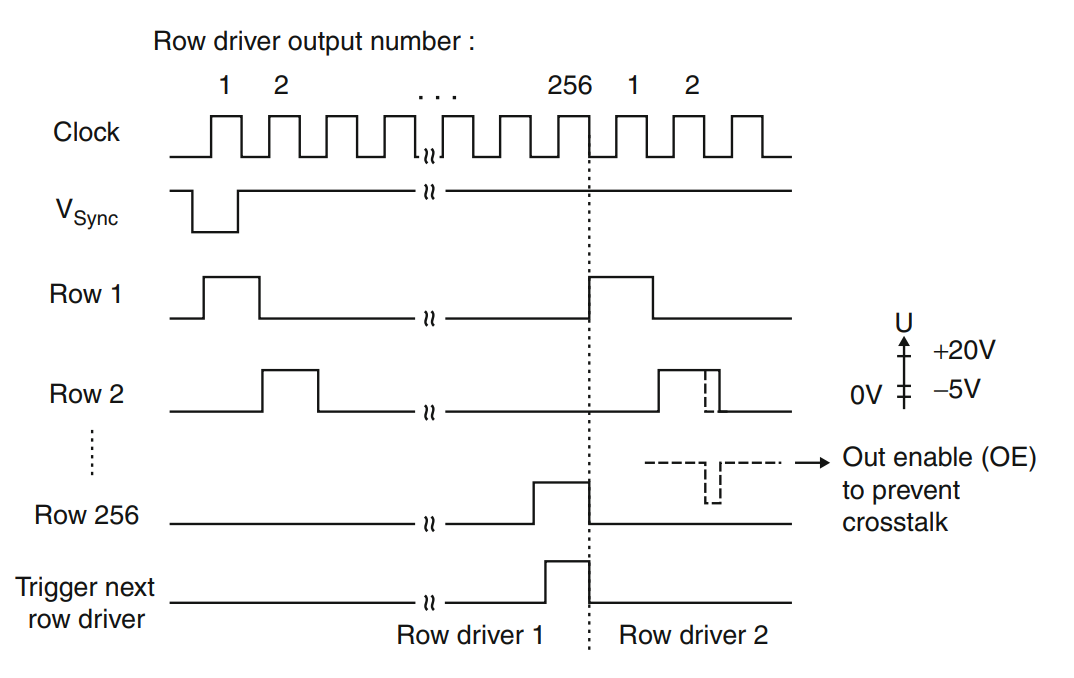
column: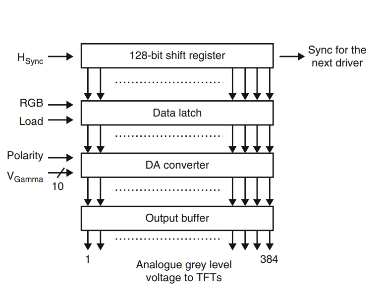
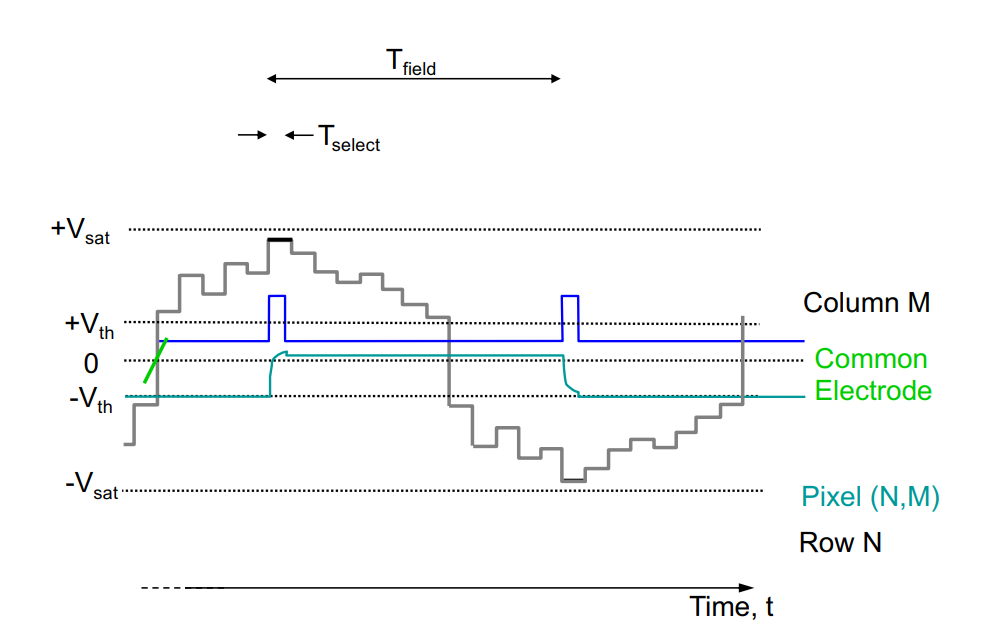
(?)
kickback(?)
Active matrix tech
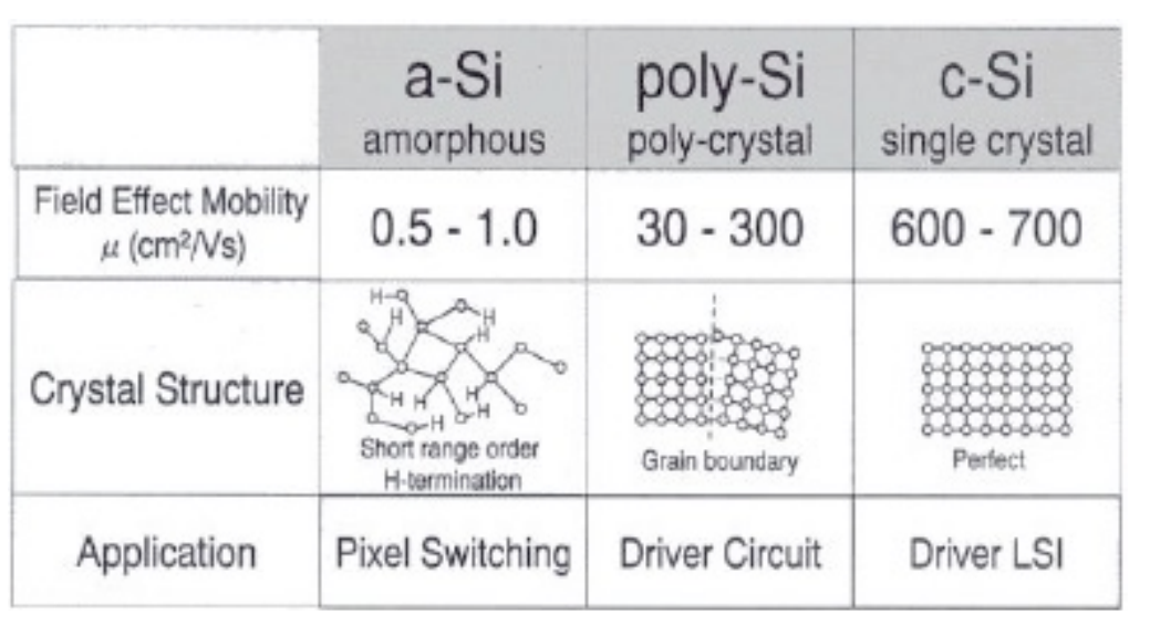
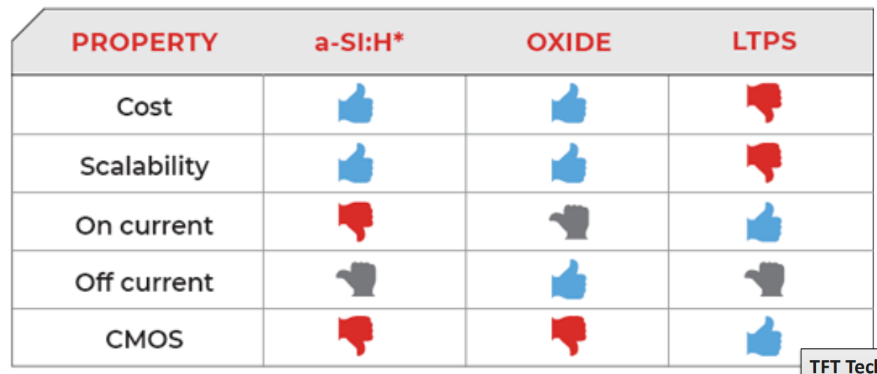
(?)
OLED structure
OLED is quite similar with LED principle, but change those structures into orginac materials
simple OLED
this is structure of simple OLED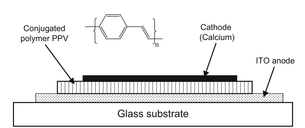
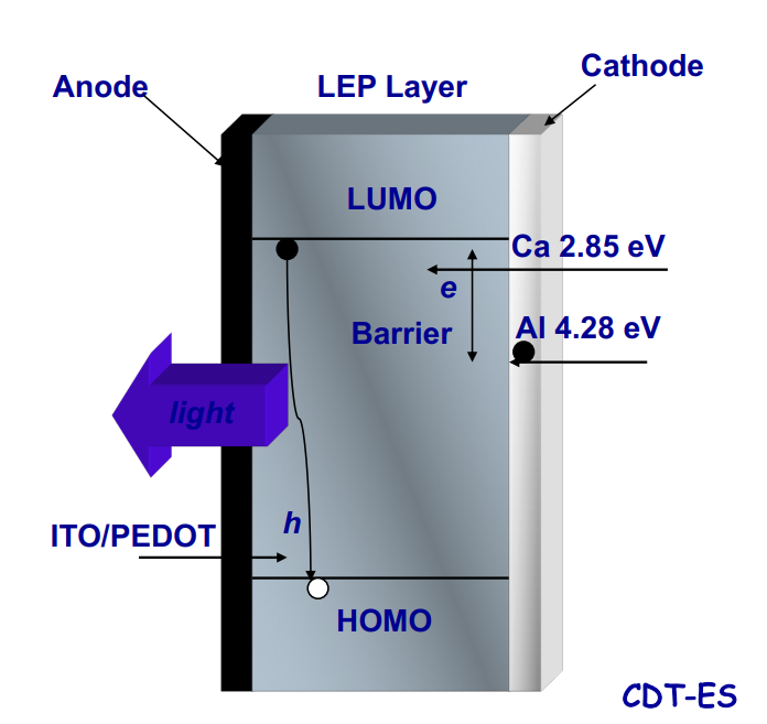
• LUMO is like valance band, HOMO is like conduction band
• Cathode assist electron injection
• Anode assist hole injection
• High mobility to reduce voltage and increase recombination probability
• emitted color is depended on energy gap
Simple Bilayer OLED Device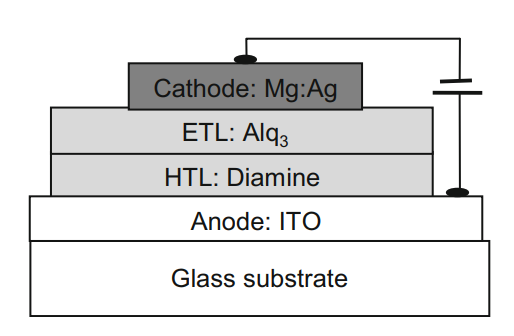
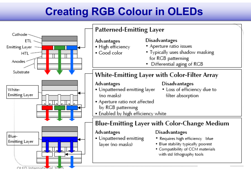
Advanced high-efficiency OLED Device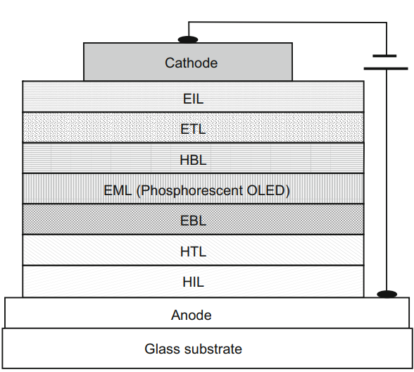
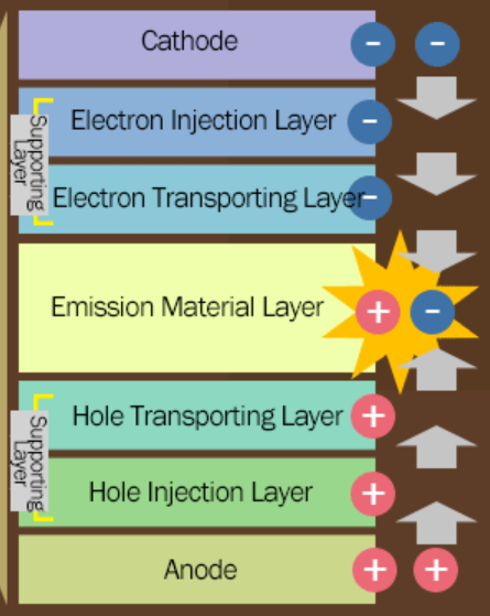
EIL(HIL): Electron (Hole) Injection layer
EIL(HIL): Electron (Hole) transport layer
EML: Emitter material layer
EBL(HBL): Electron (Hole) Block layer
bottom and top emitting: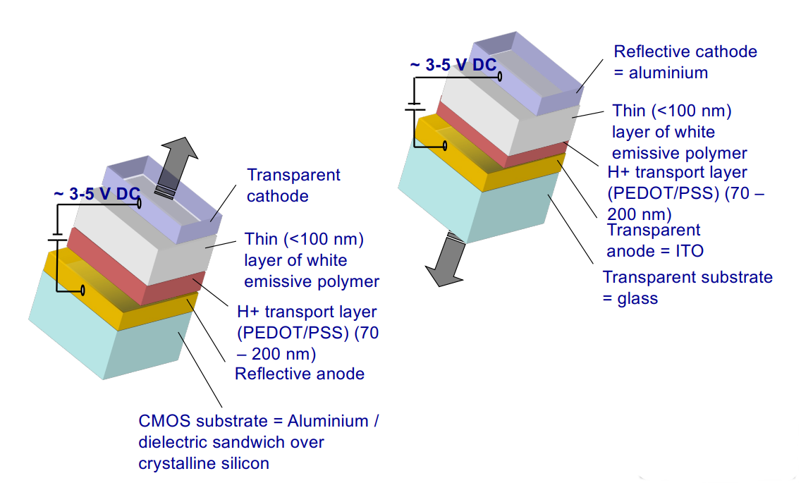
top emitter have a reflactive anode and transparent cathode
bottom emitter has a transparent anode and reflective cathode
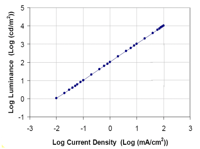
Luminance proportional to current density over many decades of dynamic range
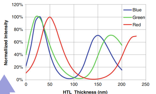
HTL’s thickness will influence final emitted light’s efficiency.
OLED image sticking problem: Pixels used more become dimmer sooner. life time, image will tuen yellow or grey

thermionic emission and tunning are two main electron/hole injection methode.
thermionic emission:
J is the emission current density,
T is the temperature of the metal,
k is the Boltzmann constant,
and A is a parameter constant
(?)
OLED zero bias, no charge injection.A (very) small current can flow due to dissociation of photo-excited excitons.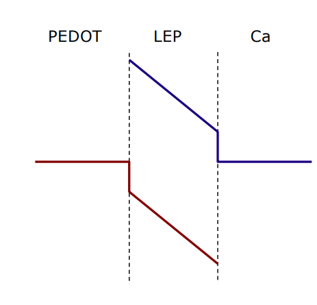
LEP: light-emitting polymer
PEDOT: poly(3,4-ethylenedioxythiophene)
threshold, OLED start to turn on, Thermionic emission allows carriers over the barriers to injection (mainly dependent on temperature)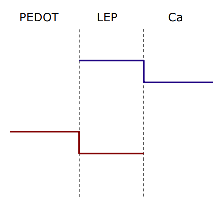
carrier injection, OLED under forward bias. current is limited by carrier injection and space charging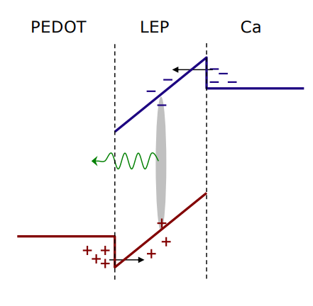
Charge Mobility µ is very low compared to inorganic semiconductors
OLED display
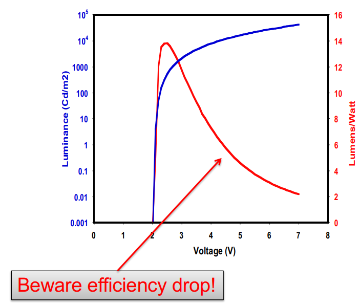
voltage-luminance relations. turn on voltage is 2.1V, luminance increases with increased voltage, but efficiency drops in hign voltage
Addressing comare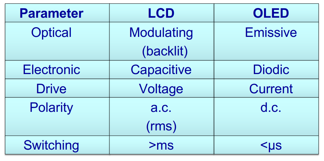
Passive matrix driver

Usually ITO anodes are ‘columns’ and Al cathodes are ‘rows’ due to the large peak currents the rows must cope with
driving method is same with passitive-matrix LCD
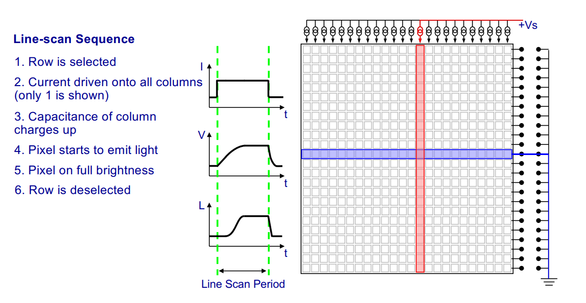
main power consumption is baed on four parts: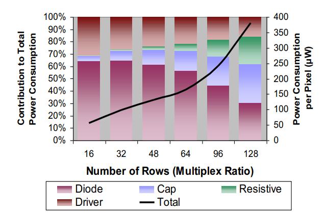
that diode (between anode and cathode) is the main consumpted part
So using more ‘standby’ or ‘pass blanklines’ can better save the power
Active matrix
use TFT control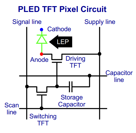
the active matrix has longer, less intense current pulse, which reduce power comsumption.
but this AMOLED have limitaitons:
- OLED luminance delay and TFT aging
- fixed pattern noise
- batch variability
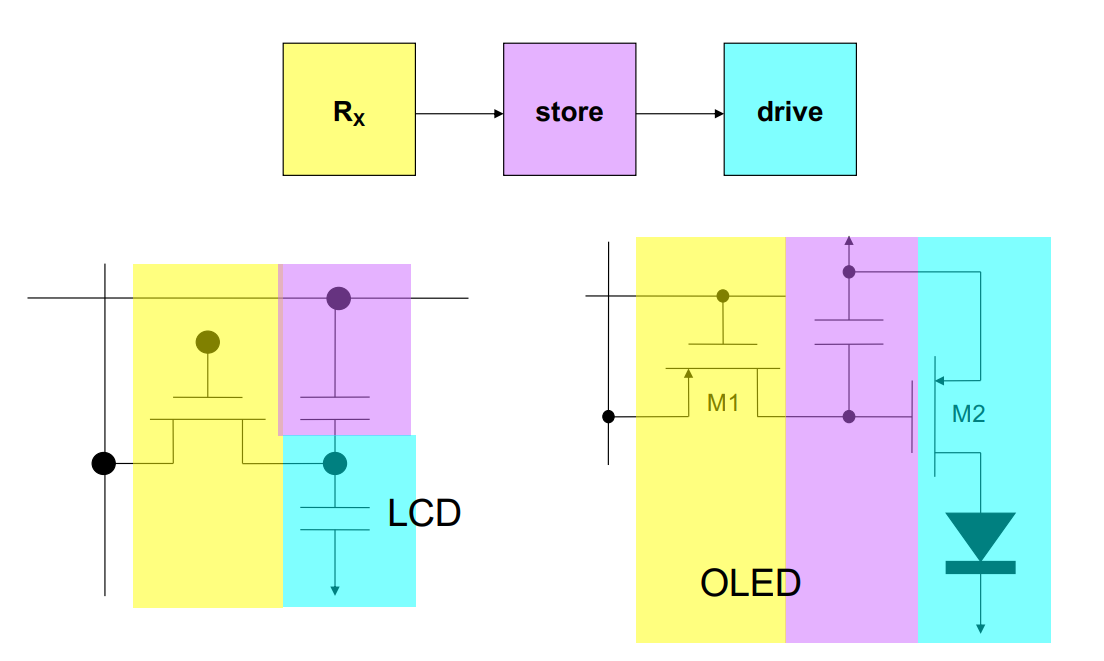
(LCD ?)
LCD is drived by voltage, and OLED is drived by current
for simple actibe-matrix OLED: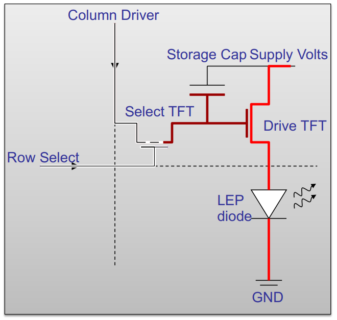
- row line is selected first, and then column is also been selected
- M1 been selected, and pass
- M2 is selected and open, drive LED
have many other sifferent designes. see them later
Micro display
the small display has:
- large image for eye
- lower manufactoe cost
- lower power consumption and battery lifetime
- often use AM-CMOS structure
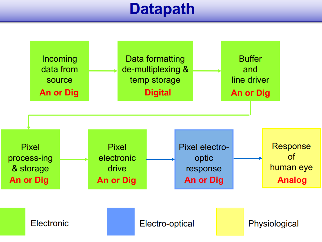
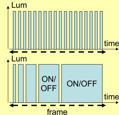
(?)
different projected methode: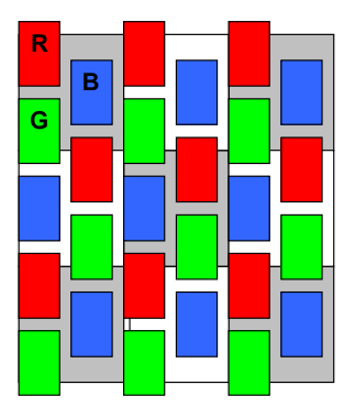
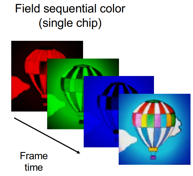
backlight is turned on in sequence, and create a final image finally
the second display method is better than first one, as scrolling methode can mix different color, but first methode is basicly has three different colors on screen.
FSC has simplier display structure, but some scence will increase color break-up if move fast
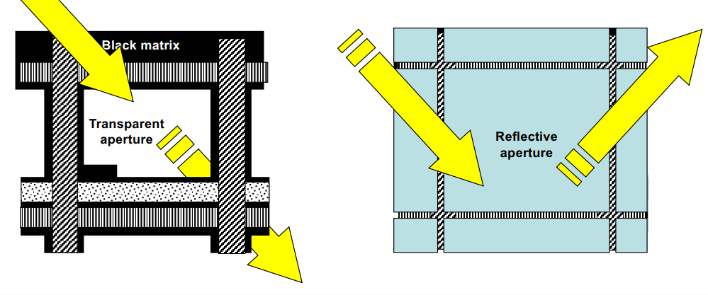
left hand is transmissive LCD, right hand is reflective LCD. the Transmissive LCD has wider side barrier, while reflective LCD has more narrower side gap.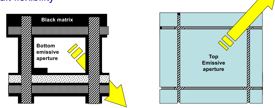
same in front/back emit OLED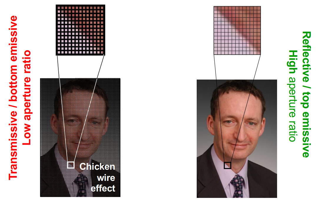
TI DMD (Digital Micromirror Device) / DLP (Digital Light Processing)
It works by using thousands of tiny mirrors that can be rapidly controlled to reflect light onto a screen, creating an image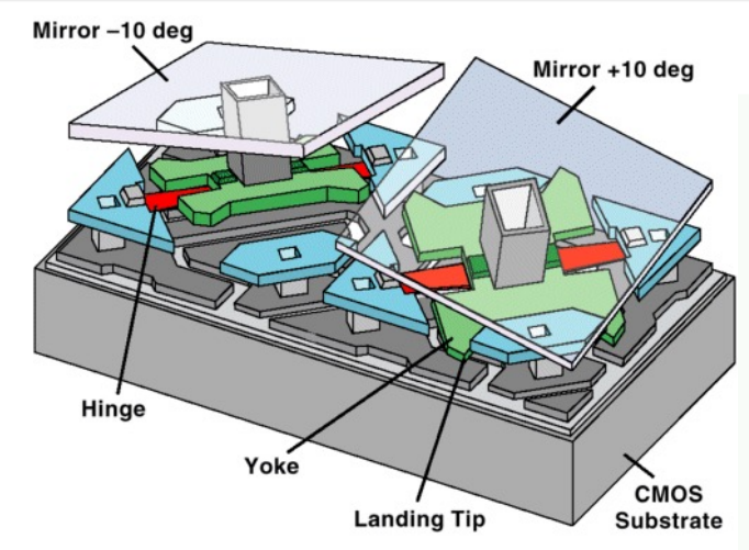
Virtual image displays
the slab glass can help change light view and outputs a virtual image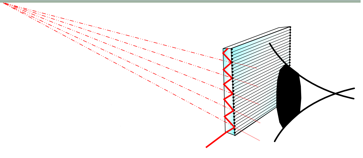
the output different angle light line can help eye create a virtual object by slab. The slab is a glass with slightly emboss one side
the angle a light line enter the salb can maintain where the seen virtual object are
we can see a file if there has a projector under this slab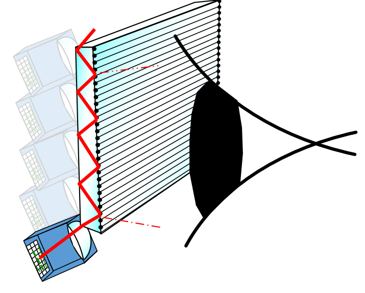
the LED need use gating ti enter the slab, to avoid diffraction due to line-width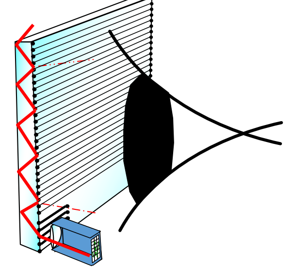
so we can create a vertical line by adding another slab, and output a full screen image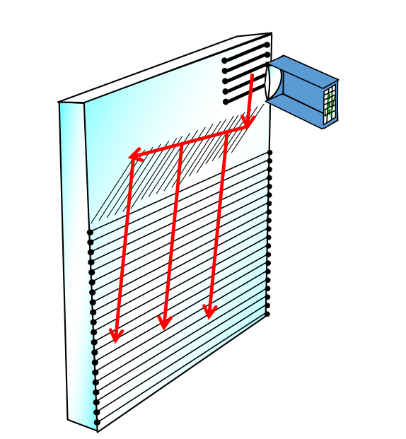
The effect of diffraction can be shown in a semi-sphere, k1 is entered light angle, k2 is diffractive direction, and kg is projected direction that entered light been diffractived.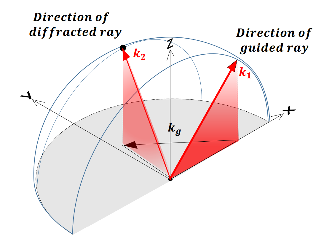
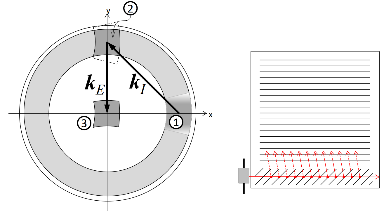
the ray angle under 42° will not be guided, and roung 90° may not hit the gating. hence 42°-72° is a good choice (projected grey ring)
1 -> 2 : first reflection
2 -> 3: second reflection
so finally ray will move to eye’s center
RGB virtual figure display. It needs three cameras due to different color’s wavelength.
this design will cause a really heavy device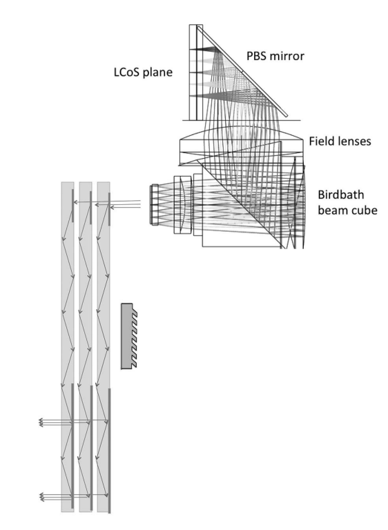
Liquid crystal photonics
LC lenses: Surface relief approach
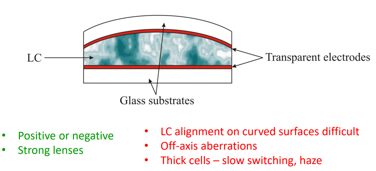
Variable index approach
Modal addressing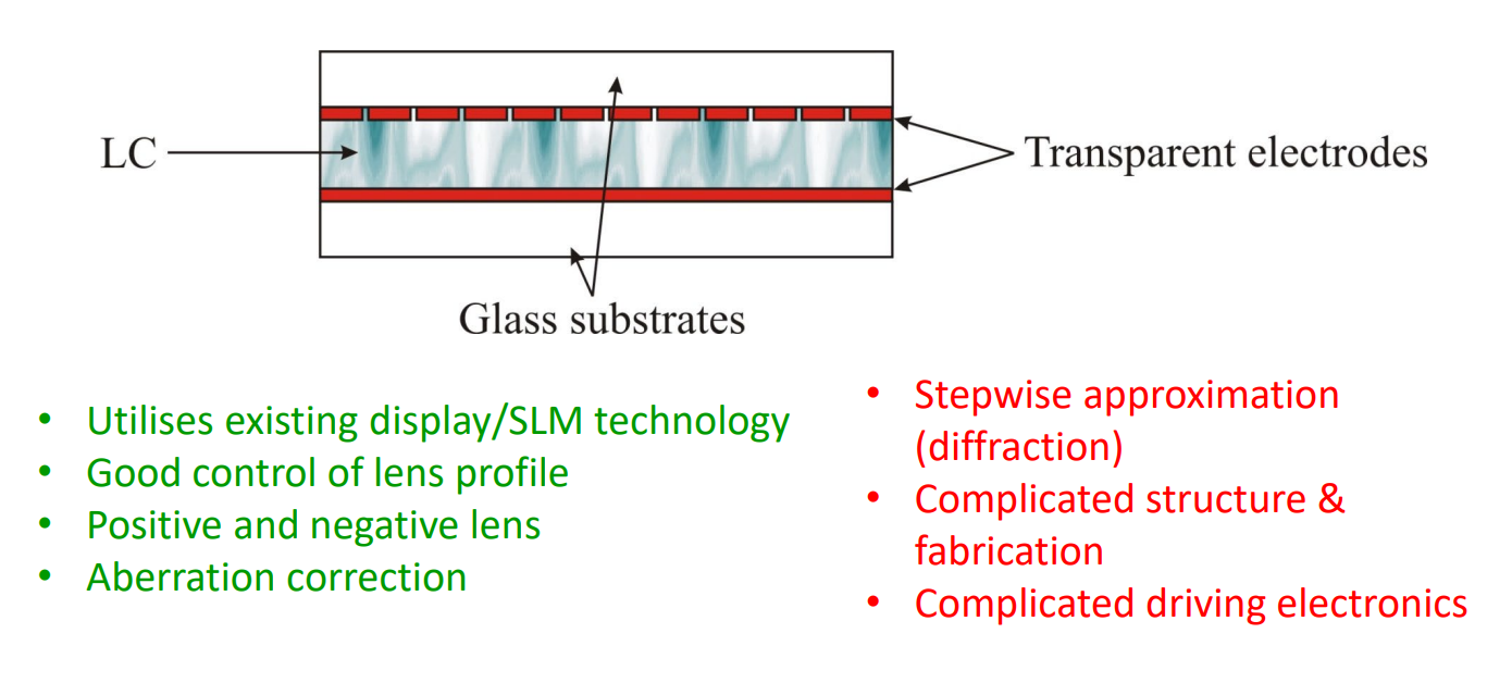
Hybrid liquid crystal lenses
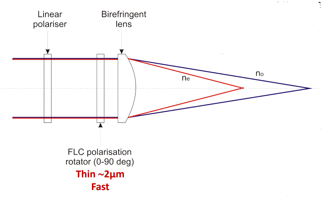
birefringence len may is the LC layer. why FLC can be rotated? change the ne/no?
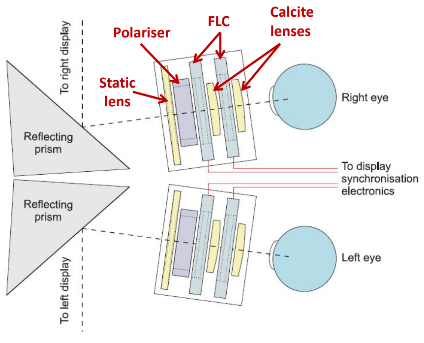
two polariser can be rotated by controller
this device can generate a 3-D virtual image
Liquid crystal lasers
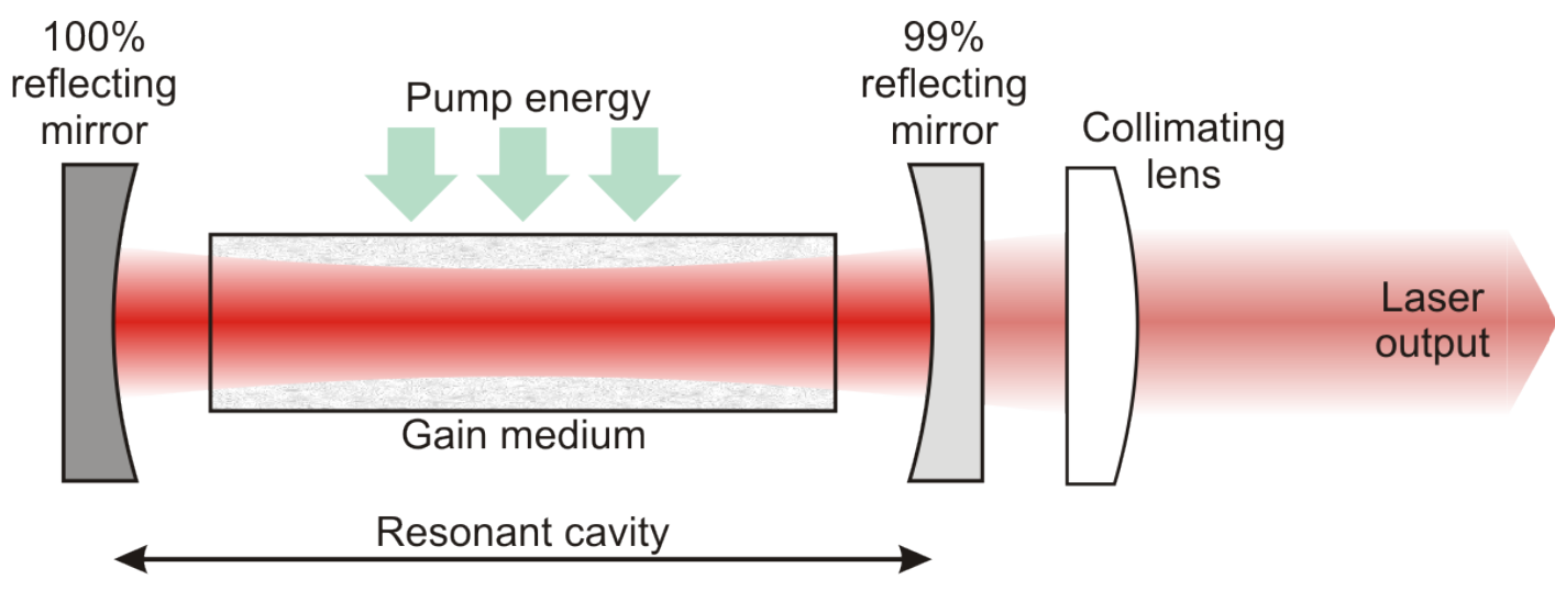
note the Resonant cavity is liquid cyrstal
if the liquid crystal is in twisted, different color waveform could be seperated using different twisted angle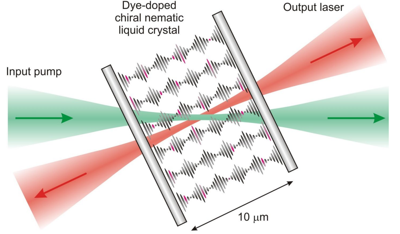
So a mixed-color laser can be seperated into multiple single-color laser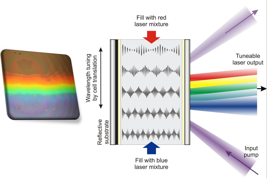
Quantum Rods LEDs
(?)